Semiconductor light emitting devices grown on composite substrates

a technology of semiconductors and light emitting devices, which is applied in the direction of semiconductor/solid-state device manufacturing, semiconductor devices, electrical devices, etc., can solve the problems of poor performance and reliability, low cost of iii-nitride substrates, and high cost of native iii-nitride substrates, so as to reduce the strain of the device

Active Publication Date: 2010-03-25
LUMILEDS
View PDF23 Cites 94 Cited by
  • Summary
  • Abstract
  • Description
  • Claims
  • Application Information

AI Technical Summary

Benefits of technology

[0003]In accordance with embodiments of the invention, a plurality of III-nitride semiconductor structures, each comprising a light emitting layer disposed between an n-type region and a p-type region, are grown on a composite substrate. The composite substrate includes a plurality of islands of III-nitride material connected to a host by a bonding layer. The...

Problems solved by technology

Since native III-nitride substrates are generally expensive and not widely available, III-nitride devices are often grown on sapphire or SiC substrates.
Such non-III-nitride substrates are less than optimal beca...

Method used


Image

  • Semiconductor light emitting devices grown on composite substrates
  • Semiconductor light emitting devices grown on composite substrates
  • Semiconductor light emitting devices grown on composite substrates

Examples


Embodiment Construction

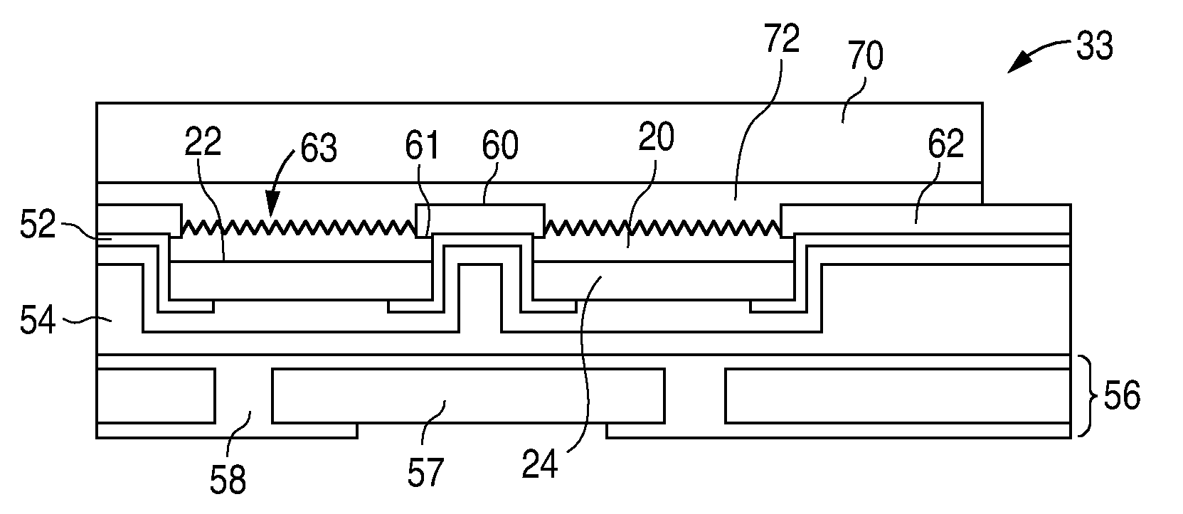
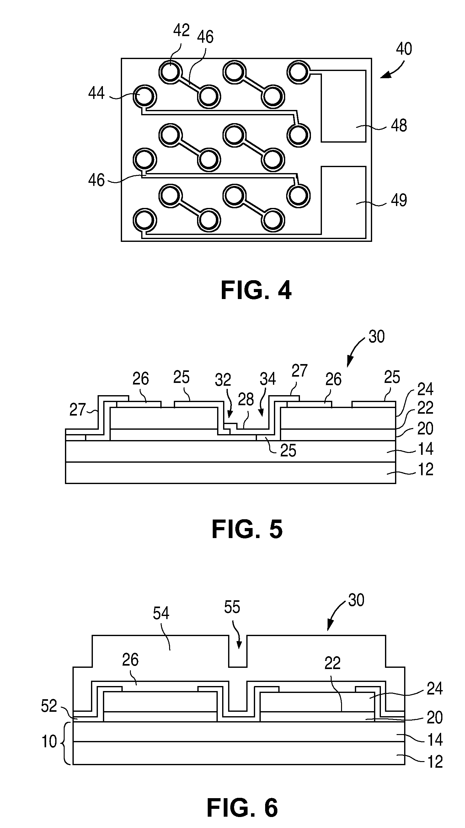
[0013]In accordance with embodiments of the invention, a III-nitride light emitting device includes a group of III-nitride structures separated by trenches. The structures may be electrically connected to form a high performance device. Such devices may be grown on composite substrates, where trenches are formed between islands of seed layer material, which trenches may improve the strain relief provided by the substrate.

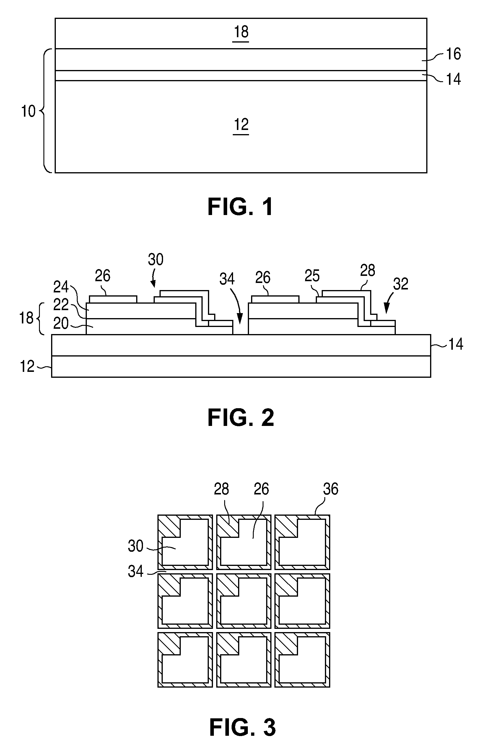
[0014]Composite substrates are described in more detail in US Patent Application Publication 2007 / 0072324, titled “Substrate for Growing a III-V Light Emitting Device” and incorporated herein by reference. An example of a composite substrate is illustrated in FIG. 1. Substrate 10 includes a host substrate 12, a seed layer 16, and a bonding layer 14 that bonds host 12 to seed 16. Each of the layers in substrate 10 are formed from materials that can withstand the processing conditions required to grow the semiconductor layers in the device. For example, in the case of...


PUM


Abstract

A plurality of III-nitride semiconductor structures, each comprising a light emitting layer disposed between an n-type region and a p-type region, are grown on a composite substrate. The composite substrate includes a plurality of islands of III-nitride material connected to a host by a bonding layer. The plurality of III-nitride semiconductor structures are grown on the III-nitride islands. The composite substrate may be formed such that each island of III-nitride material is at least partially relaxed. As a result, the light emitting layer of each semiconductor structure has an a-lattice constant greater than 3.19 angstroms.

Description

DESCRIPTION OF RELATED ART[0001]Semiconductor light-emitting devices including light emitting diodes (LEDs), resonant cavity light emitting diodes (RCLEDs), vertical cavity laser diodes (VCSELs), and edge emitting lasers are among the most efficient light sources currently available. Materials systems currently of interest in the manufacture of high-brightness light emitting devices capable of operation across the visible spectrum include Group III-V semiconductors, particularly binary, ternary, and quaternary alloys of gallium, aluminum, indium, and nitrogen, also referred to as III-nitride materials. Typically, III-nitride light emitting devices are fabricated by epitaxially growing a stack of semiconductor layers of different compositions and dopant concentrations on a sapphire, silicon carbide, III-nitride, or other suitable substrate by metal-organic chemical vapor deposition (MOCVD), molecular beam epitaxy (MBE), or other epitaxial techniques. The stack often includes one or m...

Claims


Application Information

Patent Timeline
IPC IPC(8): H01L33/00
CPCH01L27/153H01L33/007H01L33/0079H01L33/08H01L33/12H01L2224/24H01L33/385H01L33/42H01L33/505H01L33/62H01L2933/0016H01L33/382H01L27/156H01L33/0093H01L33/00
Inventor MCLAURIN, MELVIN B.KRAMES, MICHAEL R.
Owner LUMILEDS
Why Eureka
Try Eureka