Mixed orientation and mixed material semiconductor-on-insulator wafer

a semiconductor and on-insulator technology, applied in semiconductor devices, single crystal growth, chemistry apparatus and processes, etc., can solve the problem of not emitted light as efficiently

Inactive Publication Date: 2006-10-24
GLOBALFOUNDRIES INC
View PDF3 Cites 102 Cited by
  • Summary
  • Abstract
  • Description
  • Claims
  • Application Information

AI Technical Summary

Benefits of technology

[0006]In another embodiment, the disclosure is directed to a process for fabricating a semiconductor device by providing a wafer having a first semiconductor layer with a first crystalline orientation, a first insulator layer, a second semiconductor layer with a second crystalline orientation and a second insulating layer. A plurality of first and second recesses may be formed on the second insulating layer. Next, the second semiconductor layer may be epitaxially grown to fill the first recesses. Masking the filled recess and growing the first semiconductor layer to fill the second recesses enables the formation of a silicon-on-insulator device having the first and the second crystalline orientations.

Problems solved by technology

Since silicon has an indirect bandgap, it does not emit light as efficiently as semiconductor materials with a direct bandgap such as GaAs, InP, InGaAs, etc.

Method used


Image

  • Mixed orientation and mixed material semiconductor-on-insulator wafer
  • Mixed orientation and mixed material semiconductor-on-insulator wafer
  • Mixed orientation and mixed material semiconductor-on-insulator wafer

Examples


Embodiment Construction

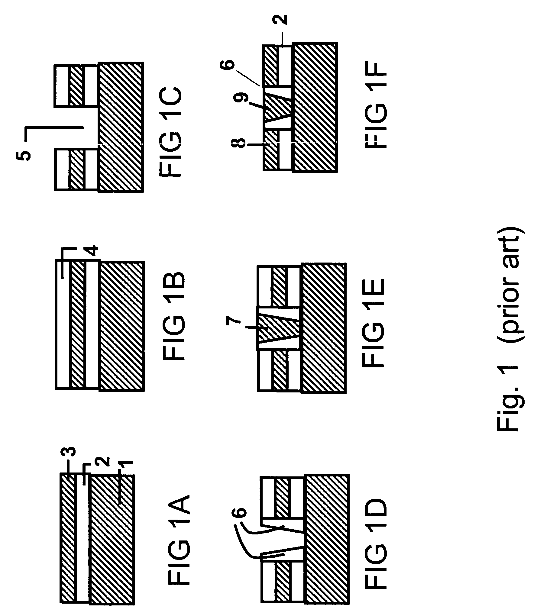
[0022]Examples of conventional approaches for producing planar hybrid substrates are shown in FIGS. 1 and 2. Referring to FIG. 1A, a silicon-on-insulator (“SOI”) wafer is prepared by interposing oxide layer 2 (buried oxide) between a handle wafer 1, having a first surface orientation (e.g., 100-orientation) and a SOI layer 3 having a second surface orientation (e.g., 110 orientation). In FIG. 1B oxide layer 4 is deposited over layer 3 as an insulation layer. In FIG. 1C, selected areas of the handle wafer are exposed by etching opening(s) 5 through layers 2–4. Dielectric sidewall spacers 6 are formed to limit silicon growth to layer 1. By allowing epitaxial silicon growth from layer 1, in FIG. 1E silicon layer 7 is formed having the same crystalline orientation as that of layer 1. The resulting structure is shown in FIG. 1F as having silicon layers 8 and 9 with different crystalline orientations and separated by oxide layer 2 and dielectric sidewall spacers 6. This approach is disadv...


PUM

PropertyMeasurementUnit
crystalline orientationaaaaaaaaaa
semiconductoraaaaaaaaaa
chemicalaaaaaaaaaa

Abstract

The present disclosure relates, generally, to a semiconductor substrate with a planarized surface comprising mixed single-crystal orientation regions and / or mixed single-crystal semiconductor material regions, where each region is electrically isolated. In accordance with one embodiment of the disclosure CMOS devices on SOI regions are manufactured on semiconductors having different orientations. According to another embodiment, an SOI device is contemplated as having a plurality of semiconductor regions having at least one of a different semiconductor material, crystalline lattice constant or lattice strain. Methods and processes for fabricating the different embodiments of the invention is also disclosed.

Description

BACKGROUND [0001]Complementary Metal Oxide Semiconductor (“CMOS”) technology is widely used for realizing semiconductor-based electronic circuits. CMOS circuits use both NMOS (electrons) and PMOS (holes) devices. Since a CMOS device-pair consumes power only during switching, CMOS chips require less power than chips using just one type of transistor. CMOS has been particularly attractive for use in battery-powered devices, such as portable computers.[0002]CMOS technology integrates both n-type and p-type MOS devices on the same wafer chip. The current of a field effect transistor (“FET”) is proportional to the carrier mobility. PFET carrier mobility is known to be 2.5 times higher on a 110-oriented silicon (Si) wafer than on a 100-oriented Si wafer. Hence, it is desirable to create a hybrid substrate comprising 100-oriented Si where NFETs would be formed and 110-oriented Si where PFET would be formed.[0003]The concept of using different orientations on the same semiconductor may be e...

Claims


Application Information

Patent Timeline
Patent Type & Authority Patents(United States)
IPC IPC(8): H01L21/20C30B1/00H01L21/36H01L21/8238H01L21/8249H01L21/84H01L27/12
CPCH01L21/84H01L27/1203H01L21/02381H01L21/02433H01L21/02532H01L21/0262H01L21/02639H01L27/1207H01L21/02647H01L21/823807
Inventor COHEN, GUY M.REZNICEK, ALEXANDERSAENGER, KATHERINE L.YANG, MIN
Owner GLOBALFOUNDRIES INC
Why Eureka
Try Eureka