Nitride-based semiconductor device

a technology of nitride and semiconductor, applied in the direction of semiconductor/solid-state device manufacturing, semiconductor devices, electrical apparatus, etc., can solve the problem of difficult nitride-based semiconductor

Active Publication Date: 2007-06-28
KK TOSHIBA
View PDF2 Cites 85 Cited by
  • Summary
  • Abstract
  • Description
  • Claims
  • Application Information

AI Technical Summary

Benefits of technology

[0013]According to one aspect of the present invention, a nitride-based semiconductor device comprising: a diode provided on a semiconductor substrate, the diode including a first nitride-based semiconductor layer made of non-doped AlXGa1-XN (0≦X<1); a second nitride-based semiconductor layer formed on the first nitride-based semiconductor layer and made of non-doped or n-type AlYGa1-YN (0<Y≦1, X<Y) having a lattice constant smaller than that of the first nitride-based semiconductor layer; a first electrode formed on the second nitride-based semiconductor layer; a second electrode formed on the second nitride-based semiconductor layer spaced from the first electrode so as to surround the first electrode; and an insulating film that covers the second nitride-based semiconductor layer below a peripheral portion of the first electrode, wherein a recess structure portion is formed by removing a part of the second nitride-based semiconductor layer at a position near the peripheral portion of the first electrode on the second nitride-based semiconductor layer, and the first electrode is formed so as to cover the second nitride-based semiconductor layer surrounded by the recess structure portion and at least a part of the insulating film formed on the recess structure portion.
[0014]According to another aspect of the present invention, a nitride-based semiconductor device comprising: a diode provided on a semiconductor substrate, the diode including a first nitride-based semiconductor layer made of non-doped AlXGa1-XN

Problems solved by technology

In other words, it is difficult for the nitride-based semiconductor device, which includes the anode electrode having the Schottky con

Method used


Image

  • Nitride-based semiconductor device
  • Nitride-based semiconductor device
  • Nitride-based semiconductor device

Examples


first embodiment

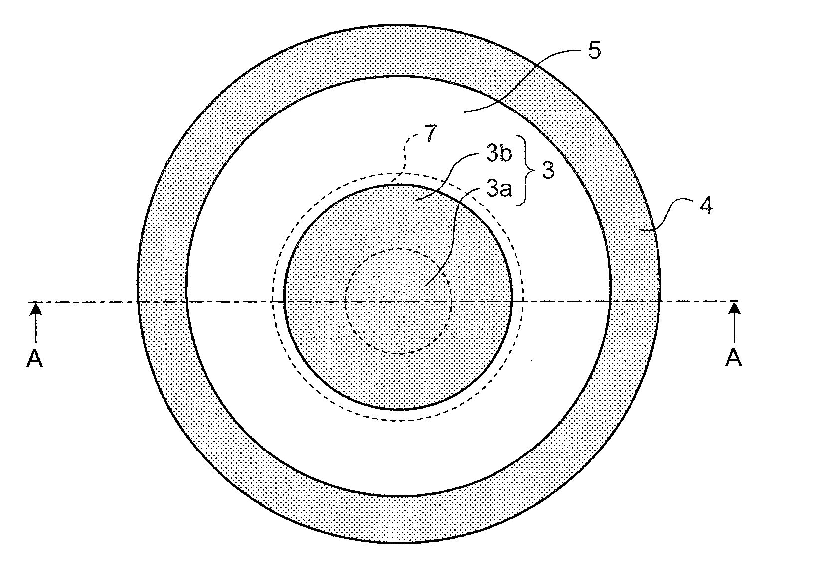
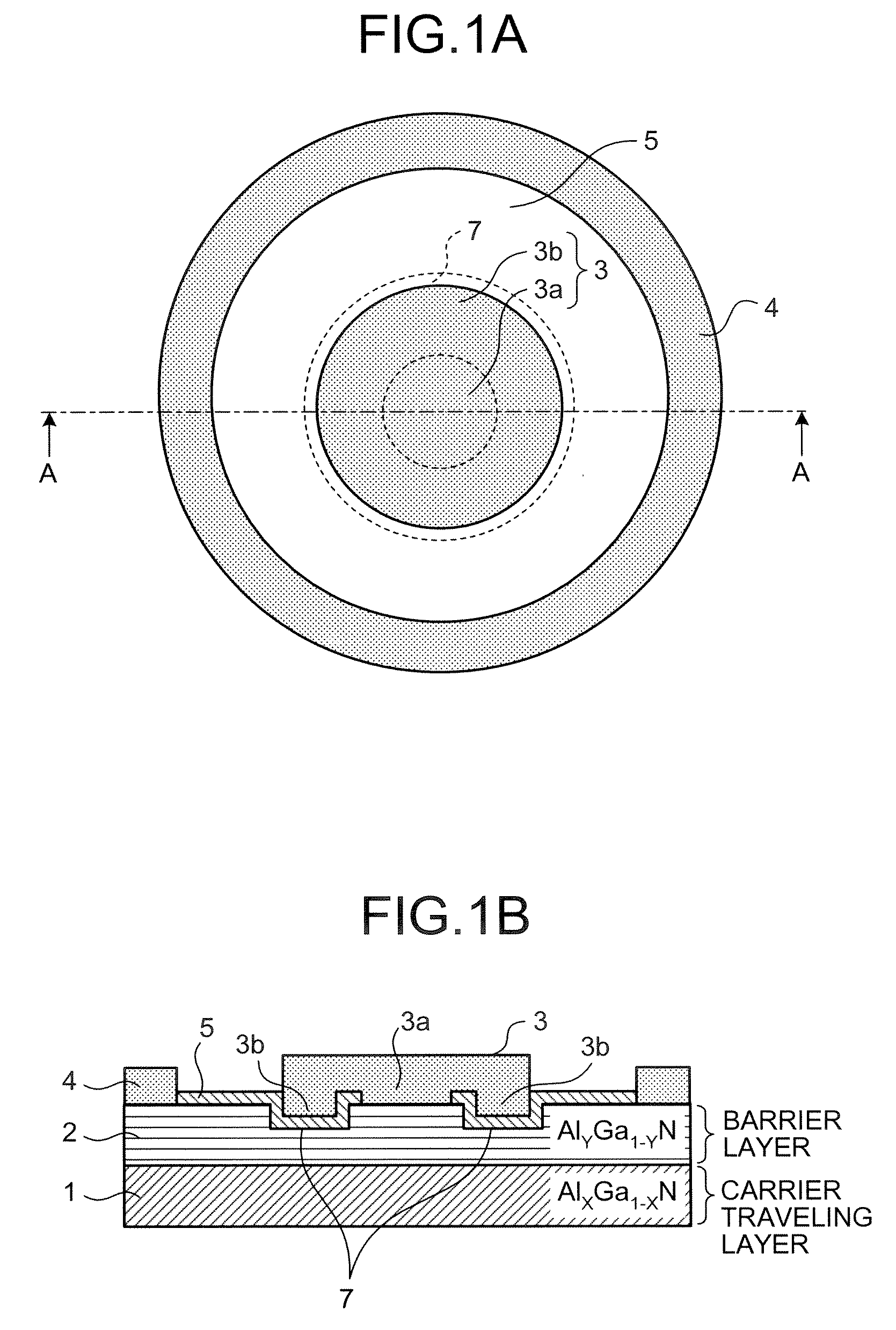
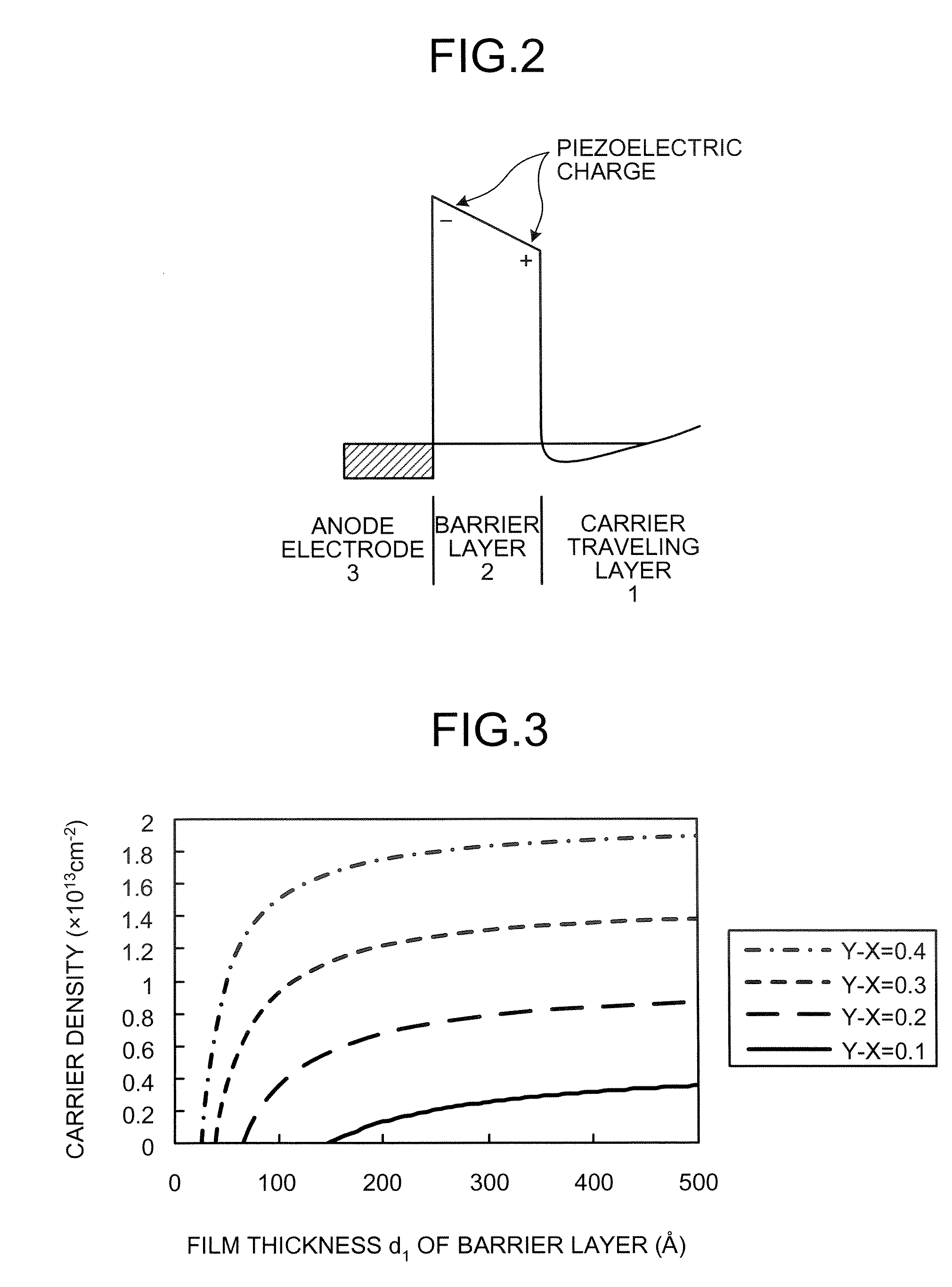
[0036]FIG. 1A is a schematic plan view of a nitride-based semiconductor device and FIG. 1B is a cross-section taken along the line A-A of FIG. 1A. The nitride-based semiconductor device is obtained by successively laminating a carrier traveling layer 1 and a barrier layer 2 on a substrate (not shown), and forming an anode electrode 3 on the barrier layer 2 and also a cathode electrode 4 thereon so as to surround the anode electrode 3. Specifically, the carrier traveling layer 1 is made of AlXGa1-XN (0≦X2 is made of AlYGa1-YN (01.

[0037]The example of FIG. 1A shows that the planar shape of the anode electrode 3 is a circle, and that the planar shape of the cathode electrode 4 is a circular ring shape formed at a position apart from a peripheral portion 3b of the anode electrode 3 by a predetermined distance so as to surround the anode electrode 3. However, any shape may be used if the cathode electrode 4 surrounds the anode electrode 3. It is noted that the carrier traveling layer 1 ...

second embodiment

[0064]FIG. 12 is a schematic cross-sectional view of a nitride-based semiconductor device according to a The planar structure of the nitride-based semiconductor device is assumed, as shown in FIG. 10, that the anode electrode 3 is surrounded by the recess structure 7 and the element separating region 8. In the nitride-based semiconductor device shown in FIG. 12, an insulating film 9 is formed over the whole surface of the nitride-based semiconductor device having the cross-sectional structure shown in FIG. 1B, and a field plate electrode 10 is formed on the insulating film 9. The cross-section of the field plate electrode 10 is such that its edge is located in between the edge of the anode electrode 3 and the edge of the cathode electrode 4 on its anode electrode 3 side.

[0065]When the anode electrode 3 of the nitride-based semiconductor device is applied with reverse bias to be turned to the off-state, the electric field concentration occurring near the anode electrode 3 is relieve...

third embodiment

[0072]The method of manufacturing the nitride-based semiconductor device, in which the diode 11 and the field effect transistor 12 shown in FIG. 13A and FIG. 13B are formed on the same substrate, is explained below. FIG. 14A to FIG. 14I are schematic cross-sectional views of one example of a procedure for the method of manufacturing the nitride-based semiconductor device according to the At first, as shown in FIG. 14A, the carrier traveling layer 1 and the barrier layer 2 are successively grown in the diode forming region RD and the transistor forming region RTR on a substrate (not shown) on which a predetermined film is formed if necessary. Specifically, the carrier traveling layer 1 is made of a non-doped AlXGa1-XN (0≦X2 is made of a non-doped or n-type AlYGa1-YN (01 and the barrier layer 2 are formed by using the epitaxial crystal growth technique such as the MOCVD method that can control the film thickness at a level of atomic layer. The film thickness of the barrier layer 2 ne...


PUM


Abstract

A nitride-based semiconductor device includes a diode provided on a semiconductor substrate. The diode contains a first nitride-based semiconductor layer made of non-doped AlXGa1-XN (0≦X<1); a second nitride-based semiconductor layer made of non-doped or n-type AlYGa1-YN (0≦Y≦1, X<Y) having a lattice constant smaller than that of the first nitride-based semiconductor layer; a first electrode formed on the second nitride-based semiconductor layer; a second electrode formed on the second nitride-based semiconductor layer; and an insulating film that covers the second nitride-based semiconductor layer below a peripheral portion of the first electrode. In the diode, a recess structure portion is formed at a position near the peripheral portion of the first electrode on the second nitride-based semiconductor layer, and the first electrode covers the second nitride-based semiconductor layer and at least a part of the insulating film.

Description

CROSS-REFERENCE TO RELATED APPLICATIONS[0001]This application is based upon and claims the benefit of priority from the prior Japanese Patent Application No. 2005-380321, filed on Dec. 28, 2005; the entire contents of which are incorporated herein by reference.BACKGROUND OF THE INVENTION[0002]1. Field of the Invention[0003]The present invention generally relates to a nitride-based semiconductor device with a diode structure and a nitride-based semiconductor device with a diode and a field effect transistor provided on a same substrate.[0004]2. Description of the Related Art[0005]A power semiconductor device such as a switching device and a diode is used for a power conversion device such as a switching power supply. A high breakdown voltage, a low on-voltage, and a low reverse-bias leak current are demanded for the power semiconductor device. To obtain the high breakdown voltage, it is effective to use a material having high critical electric field. From these facts, a nitride-based...

Claims


Application Information

Patent Timeline
IPC IPC(8): H01L33/00H01L21/28H01L21/8234H01L27/06H01L29/06H01L29/861H01L29/868
CPCH01L29/0692H01L29/2003H01L29/861H01L29/872
Inventor KURAGUCHI, MASAHIKO
Owner KK TOSHIBA
Why Eureka
Try Eureka