Scribe line structure

a line structure and scribe technology, applied in the field of scribe line structure, can solve the problems of low dielectric material looseness, weak mechanical strength structure, high infant mortality in products, etc., and achieve the effect of preventing chip cracks and raising the yield of integrated circuit chips

Inactive Publication Date: 2006-02-02
UNITED MICROELECTRONICS CORP
View PDF5 Cites 56 Cited by
  • Summary
  • Abstract
  • Description
  • Claims
  • Application Information

AI Technical Summary

Benefits of technology

[0009] It is therefore an objective of the claimed invention to provide a scribe line structure to prevent chip cracks by using laser cutting.
[0011] The claimed invention utilizes a dummy metal structure exposed in a scribe line region. Therefore, laser energy can be absorbed uniformly by the dummy metal structure when a laser beam cuts a wafer. A good heat and energy irradiative system prevents chip cracks due to lateral explosion, and raises the yield of integrated circuit chips.

Problems solved by technology

However, for achieving low dielectric property, many of low dielectric materials have loose, and weak mechanical strength structures, and are fragile.
Therefore a chip crack often occurs from lateral cutting stress while performing wafer dicing.
The chip crack causes high infant mortality in products, thereby reducing yield in subsequent electric test processes.
In addition, moisture can permeate into the integrated circuit along the chip crack to corrode the metal wires and cause the integrated circuit to break down in reliability test processes.
So this will cause the energy not only to release from bottom to top, but will also cause lateral exploding, and make chip cracks, thereby influencing product yields seriously.

Method used


Image

  • Scribe line structure
  • Scribe line structure
  • Scribe line structure

Examples


Embodiment Construction

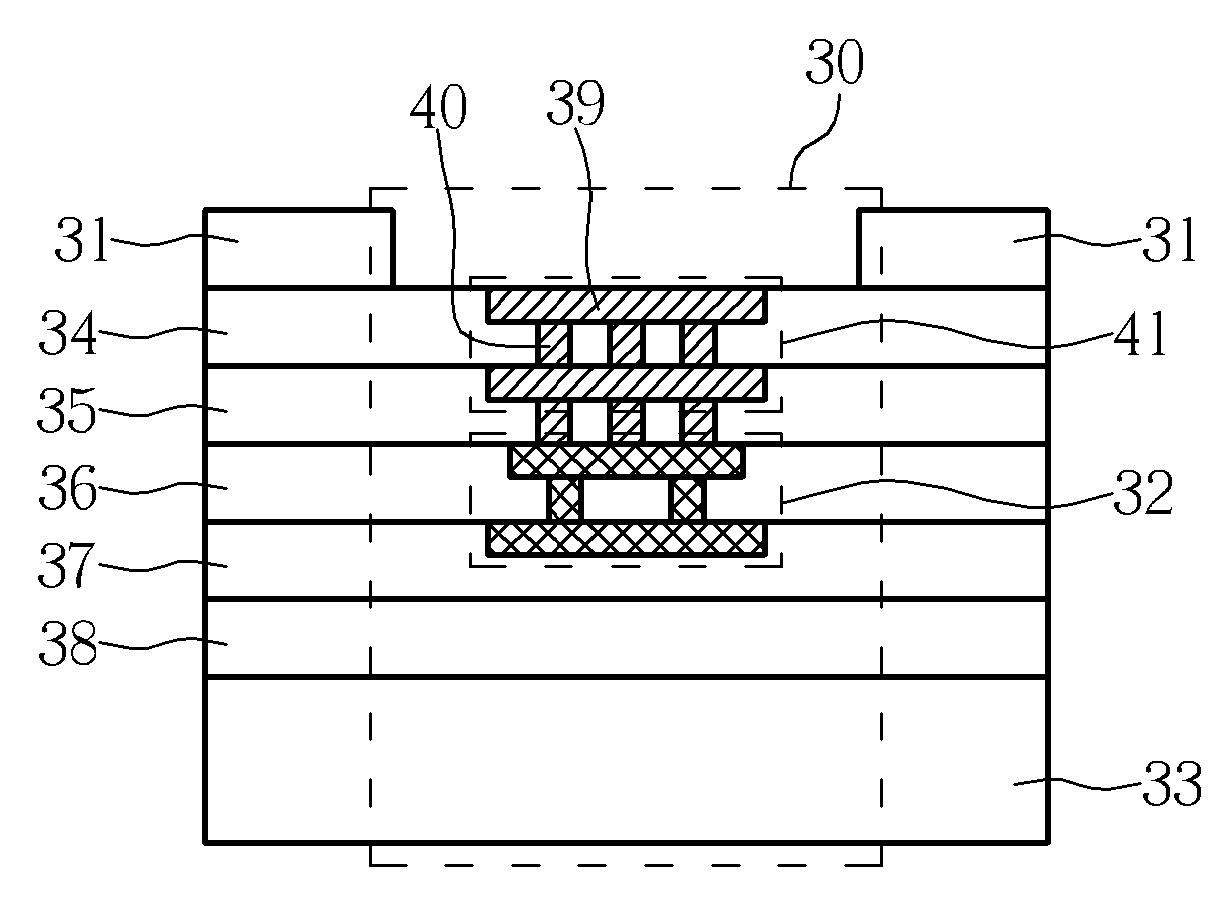
[0016] Please refer to FIG. 3. FIG. 3 is a section view of a first embodiment scribe line structure according to the present invention. As shown in FIG. 3, the bottom of the scribe line structure is a substrate 33 and a plurality of dielectric layers 34, 35, 36, 37, and 38 are formed on the substrate 33. Some of these dielectric layers 34-38 are dielectric layers having a dielectric constant less than or equal to 3 and some of them are made of other dielectric materials. Otherwise, these dielectric layers 34-38 can all be dielectric layers of low dielectric constant materials. A protection layer 31 is set on the surface of the top dielectric layer 34 and includes an open area to define a scribe line region 30.

[0017] The protection layer 31 is used to cover device regions on two sides of the scribe line region 30. The scribe line region 30 includes at least a process monitor pattern 32 made of metal material set between the dielectric layers 36 and 37. The process monitor pattern 32...


PUM

PropertyMeasurementUnit
dielectric constantaaaaaaaaaa

Abstract

The present invention provides a scribe line structure, which includes a substrate, a plurality of dielectric layers of low dielectric constant materials formed on the substrate, at least a process monitor pattern made of materials of metal formed between the dielectric layers, and a dummy metal structure connected to the process monitor pattern. The dummy metal structure includes a plurality of dummy metal layers and a plurality of dummy vias. The dummy metal structure is formed on the surface of the substrate and is exposed in the region of the scribe line, thus facilitating heat dissipation and energy release from the scribe line structure.

Description

BACKGROUND OF INVENTION [0001] 1. Field of the Invention [0002] The invention relates to a scribe line structure, and more particularly, to a scribe line structure, which utilizes a dummy metal structure to connect with process monitor patterns among a plurality of dielectric layers made out of low dielectric constant materials. [0003] 2. Description of the Prior Art [0004] The manufacturing flow of the integrated circuit can be mainly distinguish into three stages as follows: (1) the manufacturing of the wafer, (2) the fabrication of the integrated circuit, and (3) the cutting, electric testing, sorting, and packaging of the integrated circuit. When fabricating the integrated circuit on the wafer, the whole wafer is divided uniformly into many overlapping dies, and the adjacent dies are separated by a scribe line. The cutting step of the integrated circuit utilizes a cutter to cut the wafer into individual dies along the scribe lines. [0005] In recent years, the high integration se...

Claims


Application Information

Patent Timeline
Patent Type & Authority Applications(United States)
IPC IPC(8): H01L23/58
CPCH01L22/32H01L2223/54426H01L2223/5446H01L2924/0002H01L2924/00
Inventor WANG, KUN-CHIH
Owner UNITED MICROELECTRONICS CORP
Why Eureka
Try Eureka