Conductive anti-reflection coating

a technology of anti-reflection coating and conductive material, which is applied in the direction of optics, instruments, optical elements, etc., can solve the problems of complex design of conductive anti-reflection layer, large index of refraction of most transparent electrically conductive materials, and often arise design challenges, and achieve low surface contact resistance

Active Publication Date: 2006-02-02
VIAVI SOLUTIONS INC
View PDF1 Cites 11 Cited by
  • Summary
  • Abstract
  • Description
  • Claims
  • Application Information

AI Technical Summary

Benefits of technology

[0015] The instant invention relates to a conductive anti-reflection coating wherein the surface quarterwave layer is broken up into smaller portions by inserting one or more thin layers of conductive material in the dielectric material. The resulting stack of alternating layers of a dielectric material and an electrically conductive material provides a solid electrical contact to the buried conductive layer and exhibits a low surface contact resistance.

Problems solved by technology

While this is feasible in most instances, design challenges often arise when the anti-reflective coating is designed to be electrically conductive.
The index of refraction of most transparent electrically conductive materials, however, is relatively large.
It is this high index of refraction that complicates the design of conductive anti-reflection layers.
Unfortunately, these methods of reducing surface contact resistance significantly increase costs and lengthen production times. In particular, ultra-sonic soldering or welding procedures are known to cause a bottleneck in the production of conductive anti-reflection coatings.
Similarly, using a mask to create dielectric-free regions on the conductive layer is associated with expensive precision tooling and additional time-consuming steps.
For example, when the conductive and dielectric layers are deposited by vacuum evaporation, the latter process includes the additional time-consuming steps of venting the chamber after the conductive layer has been deposited, precisely applying the mask, and re-evacuating the chamber prior to depositing the surface dielectric layer.

Method used


Image

  • Conductive anti-reflection coating
  • Conductive anti-reflection coating
  • Conductive anti-reflection coating

Examples


example 1

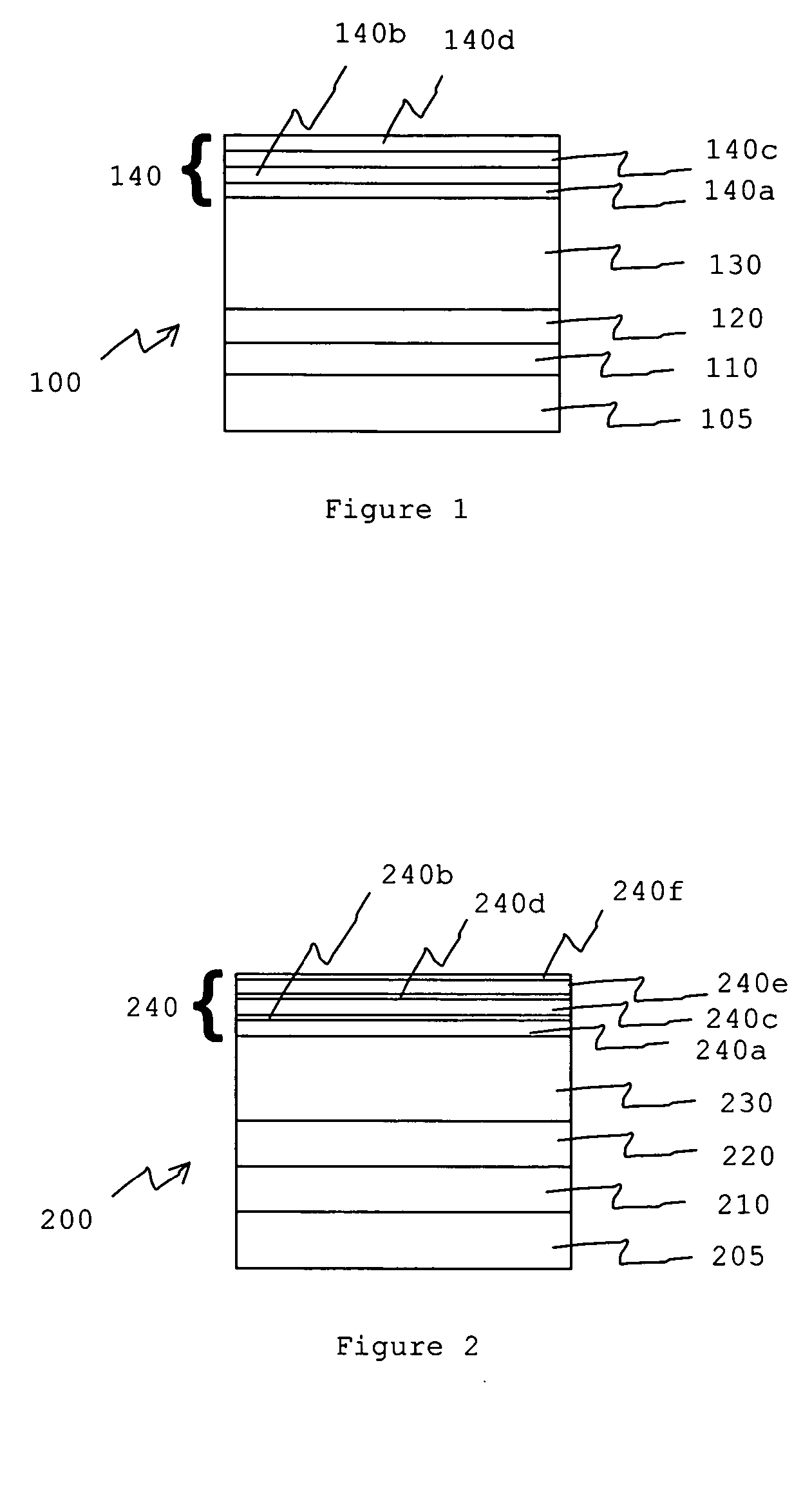
[0062] A 7-layer conductive anti-reflection coating was deposited on a Borofloat™ substrate using vacuum evaporation. More specifically, the layers were deposited according to Table 1, wherein the bottom layer (Layer 1) is in contact with the substrate and the top layer (Layer 7) is in contact with the atmosphere.

TABLE 1LayerThickness / MaterialLayer 76nm ITOLayer 628nm MgF2Layer 56nm ITOLayer 428nm MgF2Layer 3121nm ITOLayer 220nm MgF2Layer 121nm ITO

[0063] Two gold plated thin copper bus bars were bonded to the surface of the anti-reflection coating with an ACF. The measured sheet resistance was 14 ohms / square, while the surface contact resistance was about 0.24 ohms per bus bar. Notably, this surface contact resistance is sufficiently low to support EMI shielding applications.

example 2

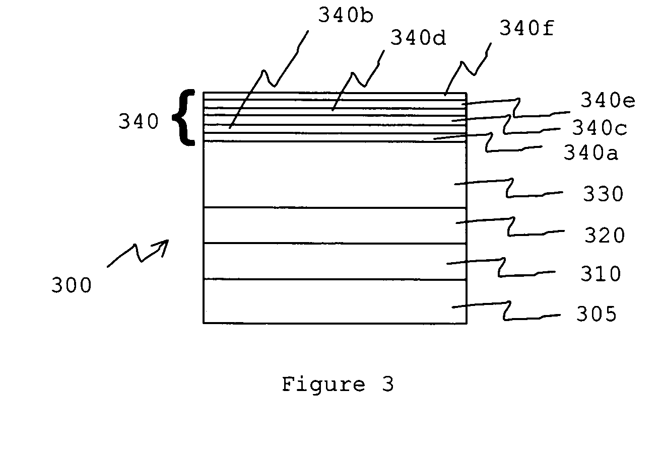
[0064] A 9-layer conductive anti-reflection coating was deposited on a Borofloat™ substrate using vacuum evaporation. More specifically, the layers were deposited according to Table 2, wherein the bottom layer (Layer 1) is in contact with the substrate and the top layer (Layer 9) is in contact with the atmosphere.

TABLE 2LayerThickness / MaterialLayer 96nm ITOLayer 814nm MgF2Layer 76nm ITOLayer 614nm MgF2Layer 56nm ITOLayer 414nm MgF2Layer 3121nm ITOLayer 220nm MgF2Layer 121nm ITO

[0065] Two gold plated thin copper bus bars were bonded to the surface of the anti-reflection coating with an ACF. The measured sheet resistance was 14 ohms / square, while the surface contact resistance was unmeasurable. Notably, this surface contact resistance is low enough to support electrical current flow in thin film resistive heaters.

example 3

[0066] A 9-layer conductive anti-reflection coating was deposited on a Borofloat™ substrate using vacuum evaporation. More specifically, the layers were deposited according to Table 3, wherein the bottom layer (Layer 1) is in contact with the substrate and the top layer (Layer 9) is in contact with the atmosphere.

TABLE 3LayerThickness / MaterialLayer 95nm ITOLayer 818nm MgF2Layer 75nm ITOLayer 618nm MgF2Layer 55nm ITOLayer 418nm MgF2Layer 3121nm ITOLayer 220nm MgF2Layer 121nm ITO

[0067] Two gold plated thin copper bus bars were bonded to the surface of the anti-reflection coating with an ACF. The measured sheet resistance was 19 ohms / square, while the surface contact resistance was unmeasurable. Notably, this arrangement was designed to minimize reflectance with respect to the anti-reflection coating shown in Example 2. In particular, the ITO layers are thinner and the MgF2 layers are thicker. Although there was an increase in the sheet resistance, due to less conductive material, th...


PUM

PropertyMeasurementUnit
thicknessaaaaaaaaaa
thicknessaaaaaaaaaa
thickaaaaaaaaaa

Abstract

A conductive anti-reflection coating has a surface quarterwave layer that is broken up into smaller portions by inserting one or more thin layers of conductive material in the dielectric material. The resulting stack of alternating layers of a dielectric material and an electrically conductive material provides a solid electrical contact to the buried conductive layer and exhibits a low surface contact resistance.

Description

CROSS-REFERENCE TO RELATED APPLICATIONS [0001] Not Applicable. MICROFICHE APPENDIX [0002] Not Applicable. TECHNICAL FIELD [0003] The present application relates generally to conductive anti-reflection coatings, and in particular, to conductive anti-reflection coatings with low surface contact resistance. BACKGROUND OF THE INVENTION [0004] Anti-reflection coatings are used extensively in optical and / or opto-electrical applications where it is often necessary to decrease reflections at an interface, such as at the boundary between air and glass. [0005] The simplest anti-reflection coating consists of a single layer of a transparent dielectric material deposited directly on a substrate. The layer of transparent dielectric material is selected such that it has an index of refraction, n, that is less than the index of refraction of the substrate, and such that it has a thickness, d, that allows the optical thickness (n times d) to be about one quarter of the central wavelength of the spe...

Claims


Application Information

Patent Timeline
Patent Type & Authority Applications(United States)
IPC IPC(8): G02F1/1335
CPCG02B1/113G02F1/13439G02F1/133502
Inventor TAKANO, KAZUAKICHURCH, ANDREW JOHNJONES, THOMAS R.TARTER, BRAD SCOTT
Owner VIAVI SOLUTIONS INC
Why Eureka
Try Eureka