Image sensor with enlarged outward appearance of microlens and method for fabricating the same

Active Publication Date: 2006-02-02
INTELLECTUAL VENTURES II
View PDF12 Cites 30 Cited by
  • Summary
  • Abstract
  • Description
  • Claims
  • Application Information

AI Technical Summary

Benefits of technology

[0029] It is, therefore, an object of the present invention to provide an image sensor capable of preventing microlens deformatio

Problems solved by technology

That is, 13% of the incident light is wasted in this case.
The above kind of limitations induce even more serious limitations as the sizes of unit pixels are being scaled down due to the large integration scale of

Method used


Image

  • Image sensor with enlarged outward appearance of microlens and method for fabricating the same
  • Image sensor with enlarged outward appearance of microlens and method for fabricating the same
  • Image sensor with enlarged outward appearance of microlens and method for fabricating the same

Examples


Example

[0042] An image sensor with an enlarged outward appearance of a microlens and a method for fabricating the same in accordance with certain embodiments of the present invention will be described in detail with reference to the accompanying drawings.

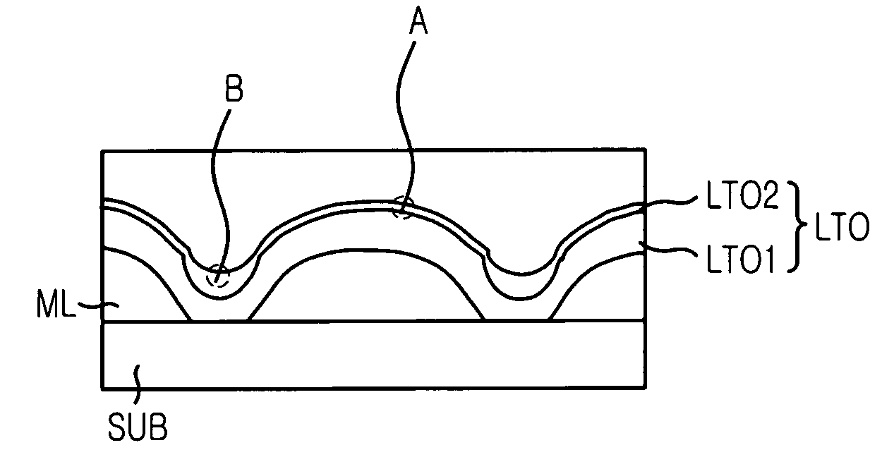
[0043]FIG. 5 is a cross-sectional view illustrating enlarged outward appearances of microlenses caused by a flowable protection layer in accordance with a specific embodiment of the present invention.

[0044] Referring to FIG. 5, although not illustrated, light receiving elements such as photodiodes, various transistors, metal wirings and color filters are formed on a substrate SUB. Also, microlenses ML are formed on the above resulting substrate structure, and a protecton layer of low temperature oxide (LTO) is formed over the microlenses ML.

[0045] According to the specific embodiment of the present invention, it is targeted to provide the LTO layer that can be formed by a low temperature process with superior step coverage. Thus, superi...


PUM


Abstract

An image sensor with an enlarged outward appearance of a microlens and a method for fabricating the same are provided. The image sensor includes: a plurality of microlenses formed on a semiconductor substrate with a certain spacing distance; and a protection layer formed over the microlenses, wherein the protection layer includes a first oxide layer which is formed by a plasma enhanced chemical vapor deposition (PECVD) method and a second oxide layer which is formed by a spin on glass (SOG) method over the first oxide layer to maintain sufficient step coverage over chasms between the microlenses.

Description

FIELD OF THE INVENTION [0001] The present invention relates to an image sensor and a method for fabricating the same; and, more particularly, to an image sensor including a protection layer for a microlens and a method for fabricating the same. DESCRIPTION OF RELATED ARTS [0002] An image sensor is a semiconductor device which converts an optical image to an electric-signal, and a charge coupled device (CCD) and a complementary metal-oxide-silicon (CMOS) are examples of the image sensor. [0003] The CCD is a semiconductor device, which transfers and stores charge carriers into metal-oxide-silicon (MOS) capacitors located very closely to each other. [0004] On the other side, the CMOS image sensor is a semiconductor device which employs a switching method. The switching method forms MOS transistors in the same number as pixels by utilizing CMOS technology which uses a control circuit and a signal processing circuit as a peripheral circuit, and employs the MOS transistors to detect outpu...

Claims


Application Information

Patent Timeline
IPC IPC(8): G02B27/10
CPCG02B3/0018H01L27/14685H01L27/14627G02B3/0056H01L27/146H01L31/10
Inventor KIM, SI-BUM
Owner INTELLECTUAL VENTURES II
Why Eureka
Try Eureka