Method of fabricating carbon nanotube field-effect transistors through controlled electrochemical modification

a field-effect transistor and carbon nanotube technology, applied in nanotechnology, nanoinformatics, electric instruments, etc., can solve the problems of affecting adjacent semiconducting tubes in a negative way, unable to achieve 100% separation of metallic nanotubes from semiconducting ones, etc., to achieve the effect of improving the performance of existing fets, reducing current carrying capacity, and improving the performance of existing

Inactive Publication Date: 2006-02-02
MAX PLANCK GESELLSCHAFT ZUR FOERDERUNG DER WISSENSCHAFTEN EV
View PDF2 Cites 12 Cited by
  • Summary
  • Abstract
  • Description
  • Claims
  • Application Information

AI Technical Summary

Benefits of technology

[0013] A particular object of the invention is to provide a method of obtaining FETs in which metallic SWCNTs no longer pose a problem and indeed without any substantial negative effect on the semiconducting SWCNTs.
[0030] Preferably, the chemical used in step (d) includes a diazonium salt. The use of a diazonium salt leads to an electrochemical modification of the semiconducting nanotubes according to a reductive coupling scheme if OFF state ECM is performed. In this case of reductive ECM based on a diazonium salt it is assumed that reductively created phenyl radicals form covalent (C—C) bonds to the nanotube, associated with the introduction of a sizable density of sp3-hybridized carbon atoms. This reductive diazonium coupling to metallic SWCNTs increases the resistance of the SWCNT by up to four orders of magnitude.

Problems solved by technology

In contrast to the remarkable achievements made with devices based upon individual SWCNTs, the use of nanotubes in large-scale electronics still faces several limitations which arise from the fact that all fabrication procedures developed to date yield mixtures of metallic and semiconducting tubes.
However, in none of these techniques can a 100% separation of the metallic nanotubes from the semiconducting ones be achieved, which is mainly due to the fact that the methods used are not selective exclusively to either the metallic or the semiconducting tubes.
This destructive approach which has until now successfully been applied to individual SWCNT bundles has the disadvantage that adjacent semiconducting tubes may be affected in a negative way.
Specifically, high current densities in the metallic nanotubes can heat up adjacent semiconducting tubes in the bundle thereby inducing defects in the semiconducting SWCNTs which can deteriorate device parameters such as charge carrier mobility.

Method used


Image

  • Method of fabricating carbon nanotube field-effect transistors through controlled electrochemical modification
  • Method of fabricating carbon nanotube field-effect transistors through controlled electrochemical modification
  • Method of fabricating carbon nanotube field-effect transistors through controlled electrochemical modification

Examples


Embodiment Construction

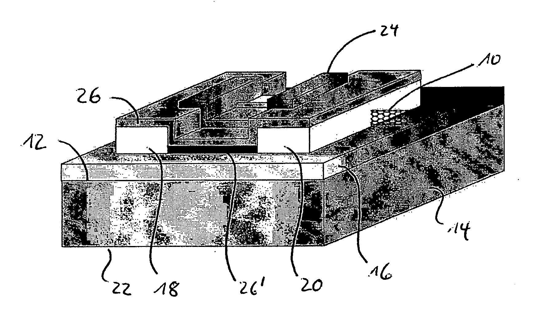
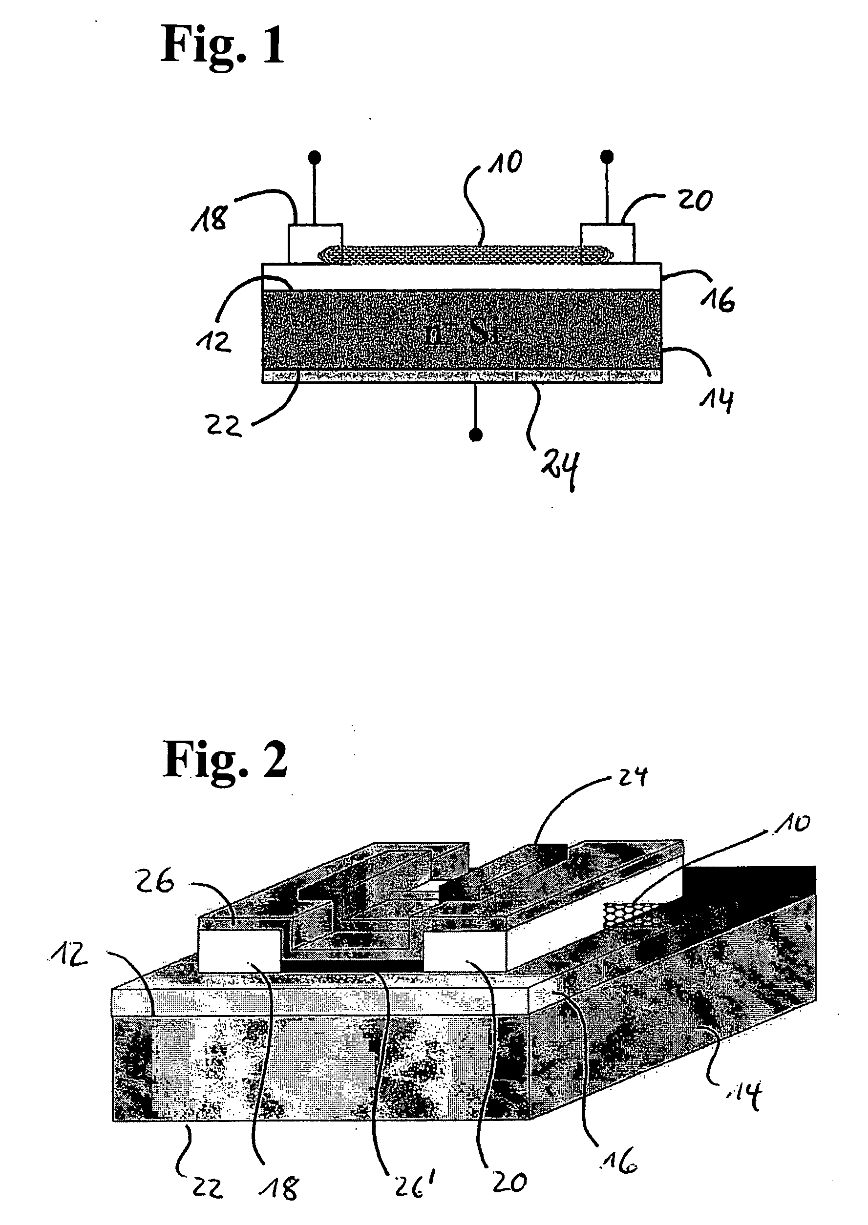
[0038] A single-wall carbon nanotube field-effect transistor (SWCNT-FET) as shown in FIG. 1 is fabricated by dispersing single-wall carbon nanotubes (SWCNTs) 10, for instance produced by the HiPCO process (high pressure pyrolysis of carbon monoxide) as performed by Tubes@Rice, Lexington, in a surfactant solution and depositing these on a substantially flat front surface 12 of an N+-doped silicon substrate 14 which is covered by a 200 nm thick layer 16 of thermally grown silicon oxide.

[0039] If the surfactant solution containing the SWCNTs 10 is poured on a substrate 14 having a flat surface 12 the nanotubes 10 typically arrange themselves with random orientation. In contrast, a predetermined orientation of the SWCNTs can be achieved by, for instance, providing the substrate with a periodic structure comprising peaks and valleys preferably extending in parallel to each other. When the surfactant solution containing the SWCNTs is distributed across a so patterned surface the SWCNTs w...


PUM

PropertyMeasurementUnit
thicknessaaaaaaaaaa
thicknessaaaaaaaaaa
thicknessaaaaaaaaaa

Abstract

The invention relates to a method of fabricating a structure with field effect transistors, said transistors each comprising a source electrode, a drain electrode, a channel extending between the source and drain electrodes and at least one gate electrode associated with the channel for controlling the conductance of the channel, wherein the channel comprises one or more semiconducting single-wall carbon nanotubes. The method includes the steps of a) depositing a plurality of single-wall carbon nanotubes on a substrate, said carbon nanotubes comprising a mixture of metallic carbon nanotubes and semiconducting carbon nanotubes, b) providing before or after step a) source and drain electrodes on the substrate so that one or more carbon nanotubes extend between the source and drain electrodes, c) applying a variable gate voltage to switch off the semiconducting tubes extending between the source and drain electrodes, d) wetting the surface of the structure including the transistors with a chemical to achieve a chemical bond between a radical supplied by said chemical and some carbon atoms of the metallic nanotubes, whereby these metallic nanotubes become non-conductive.

Description

BACKGROUND OF THE INVENTION [0001] 1. Field of the Invention [0002] The present application relates to a method of fabricating a structure with field-effect transistors, said transistors each comprising a source electrode, a drain electrode, a channel extending between source and drain electrode and at least one gate electrode associated with the channel for controlling the conductance of the channel, wherein the channel comprises one or more semiconducting single-wall carbon nanotubes. [0003] 2. Prior Art [0004] Single-wall carbon nanotubes (SWCNTs) are prospective components of nanoscale and molecular electronic devices. For instance, field-effect transistors (FETs) have been successfully fabricated from single semiconducting SWCNTs. The overall performance of SWCNT-FETs has been reported to be superior to that of state-of-the-art silicon based MOSFETs, as reflected in the values of the drive current and transconductance being higher by a factor of four. Moreover, devices implemen...

Claims


Application Information

Patent Timeline
Patent Type & Authority Applications(United States)
IPC IPC(8): H01L21/337H01L21/3205
CPCB82Y10/00H01L51/0006Y10S977/847H01L51/0512H01L51/0545H01L51/0048H10K71/125H10K85/221H10K10/462H10K10/466
Inventor BALASUBRAMANIAN, KANNANBURGHARD, MARKOKERN, KLAUS
Owner MAX PLANCK GESELLSCHAFT ZUR FOERDERUNG DER WISSENSCHAFTEN EV
Why Eureka
Try Eureka