

Integrated circuit device and testing device
- Summary
- Abstract
- Description
- Claims
- Application Information
AI Technical Summary
Benefits of technology
Problems solved by technology
Method used
Image

Examples
Embodiment Construction
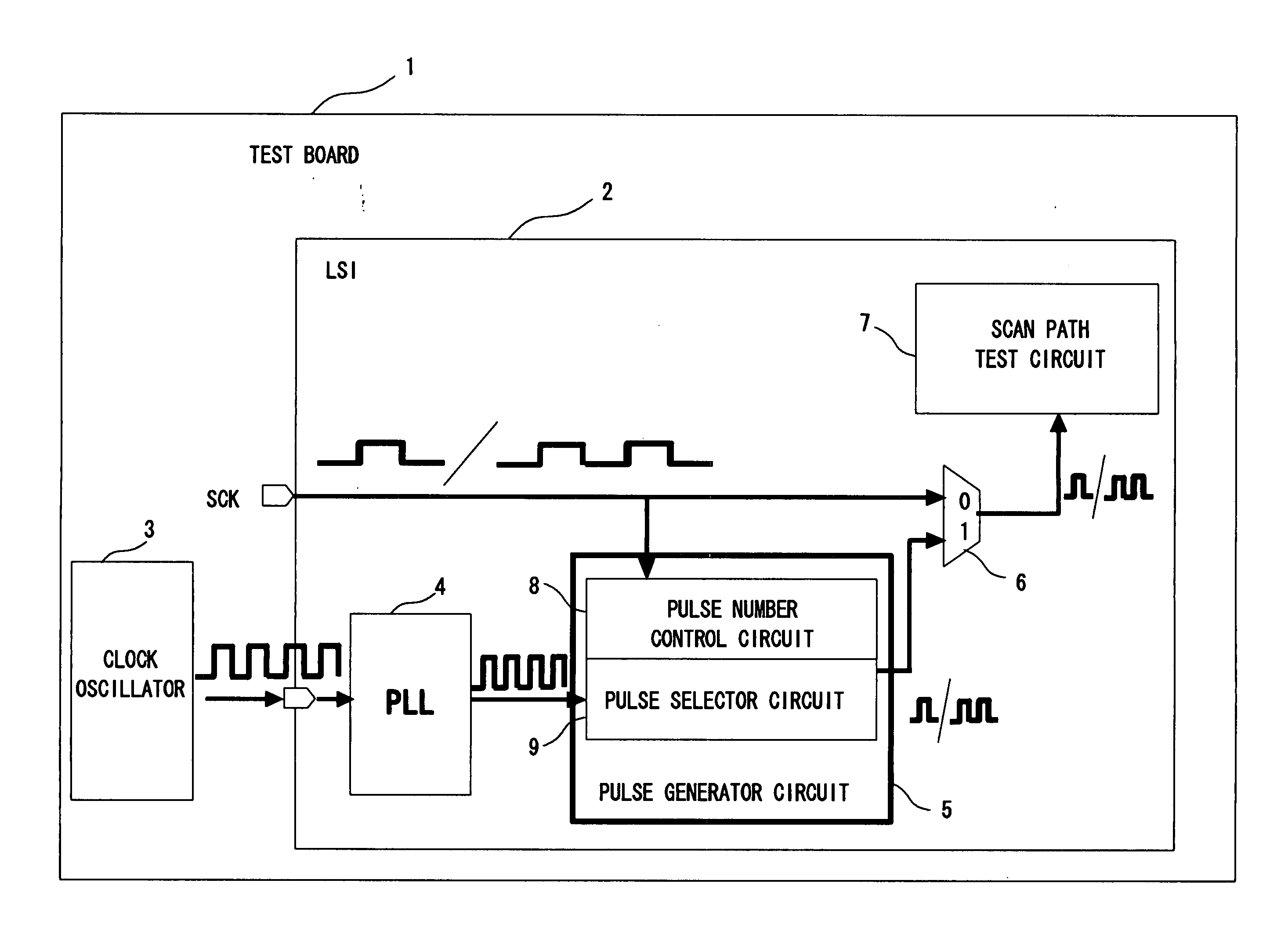
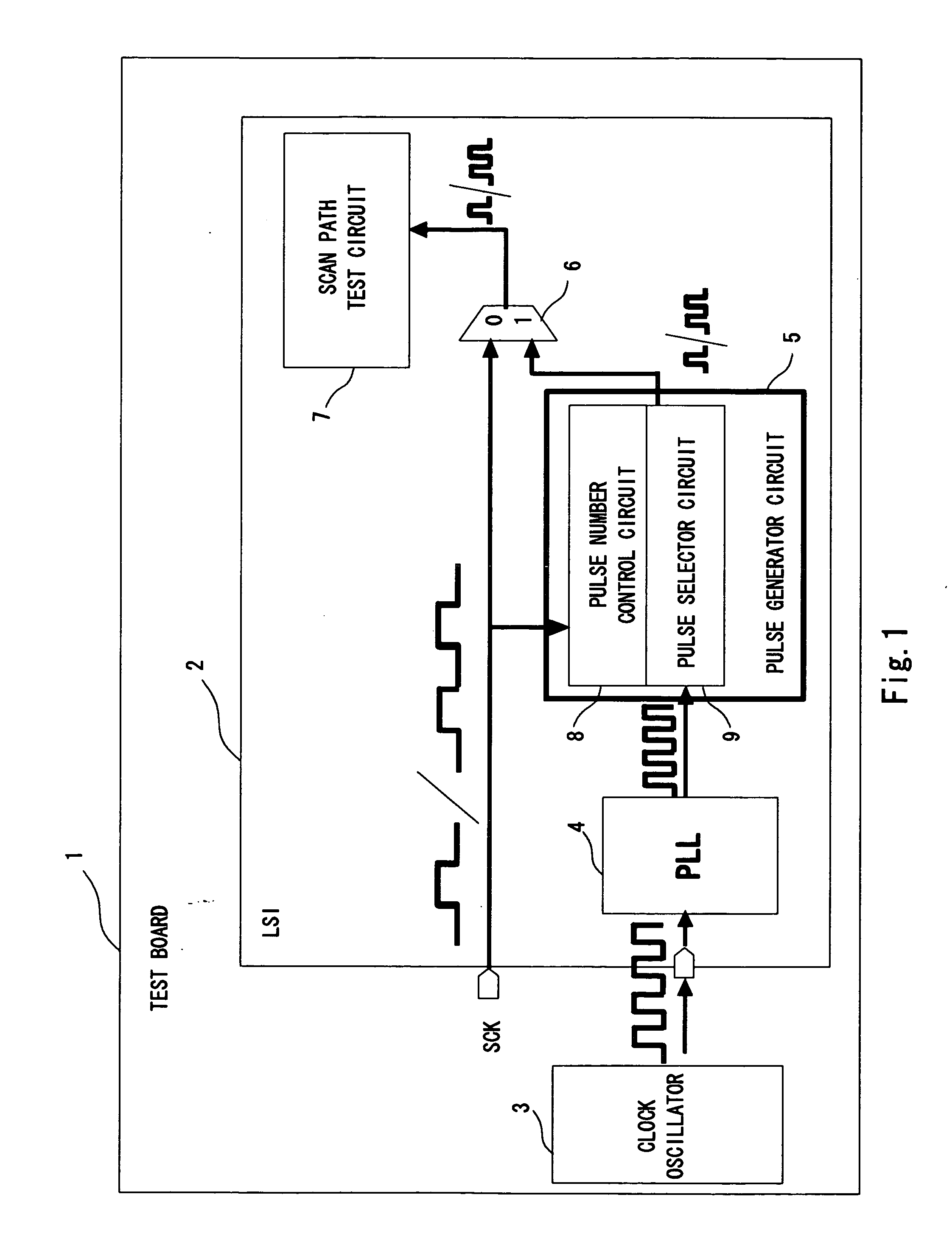
[0038] The configuration of an LSI testing device according to an embodiment of the invention is described hereinafter with reference to the block diagram of FIG. 1. The LSI testing device performs a delay test using scan path technique. Even when a tester can only generate a low frequency clock, the device can generate a high frequency clock inside the LSI and conduct a desired delay test.
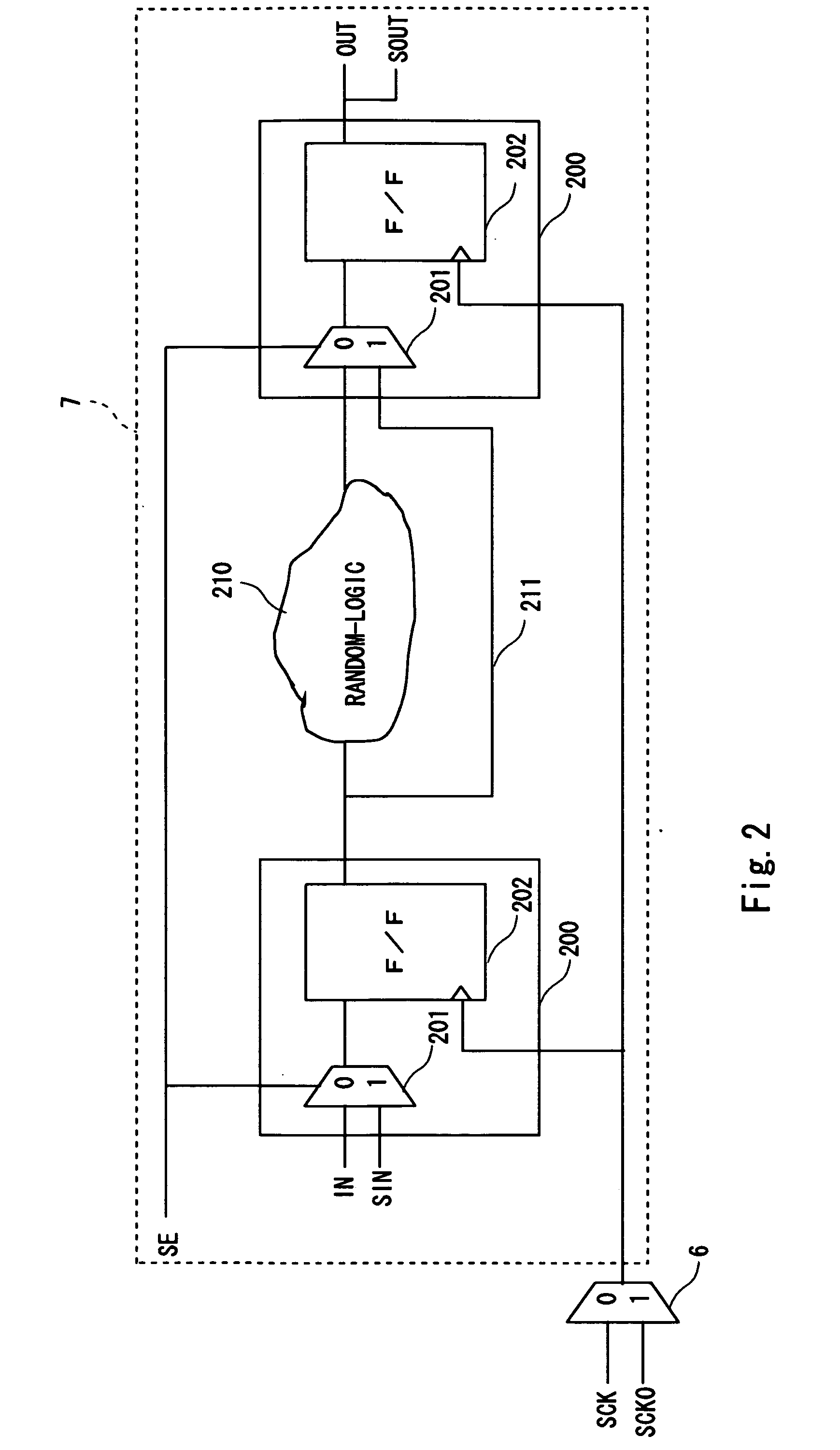
[0039] As shown in FIG. 1, the LSI testing device has a test board 1, an LSI 2 detachably mounted on the test board 1, and a clock oscillator 3 mounted on the test board 1. The LSI 2 has a PLL 4, a pulse generator circuit 5, a multiplexer 6, and a scan path test circuit 7.
[0040] The LSI 2 also has terminals for inputting a scan clock SCK and a test clock of the clock oscillator 3. Further, though not shown in FIG. 1, it has other terminals such as a scan-in terminal SIN for inputting a test pattern, a scan-out terminal SOUT for outputting a test operating result, and a scan mode control terminal...
PUM
 Abstract
Description
Claims
Application Information