

Semiconductor storage device and method of manufacturing same
- Summary
- Abstract
- Description
- Claims
- Application Information
AI Technical Summary
Benefits of technology
Problems solved by technology
Method used
Image

Examples
Embodiment Construction
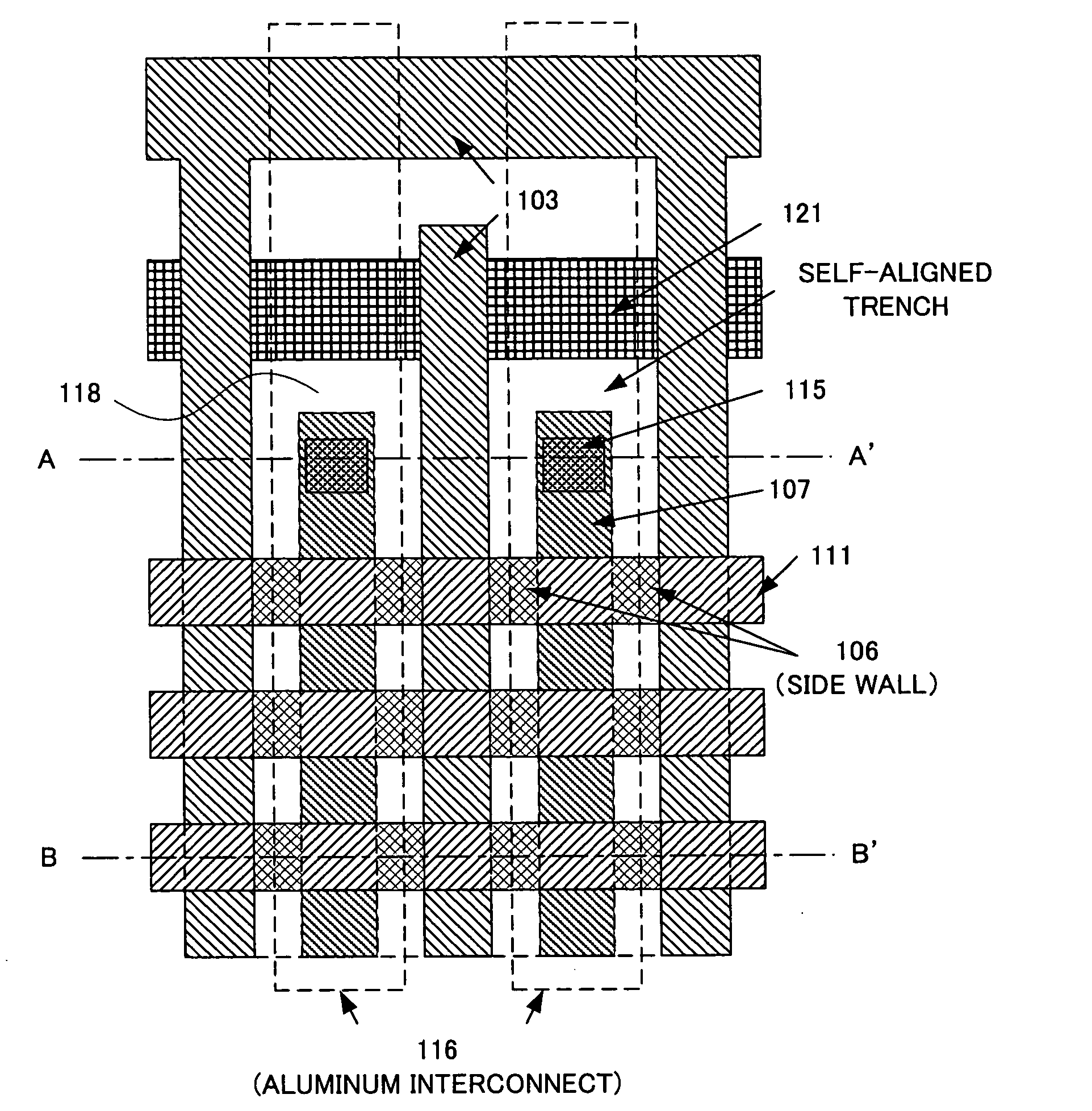
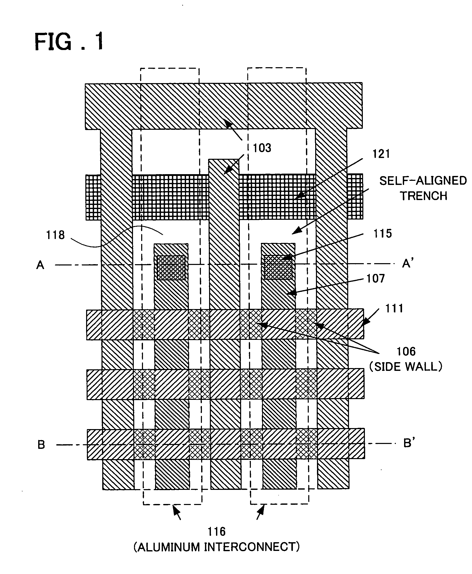
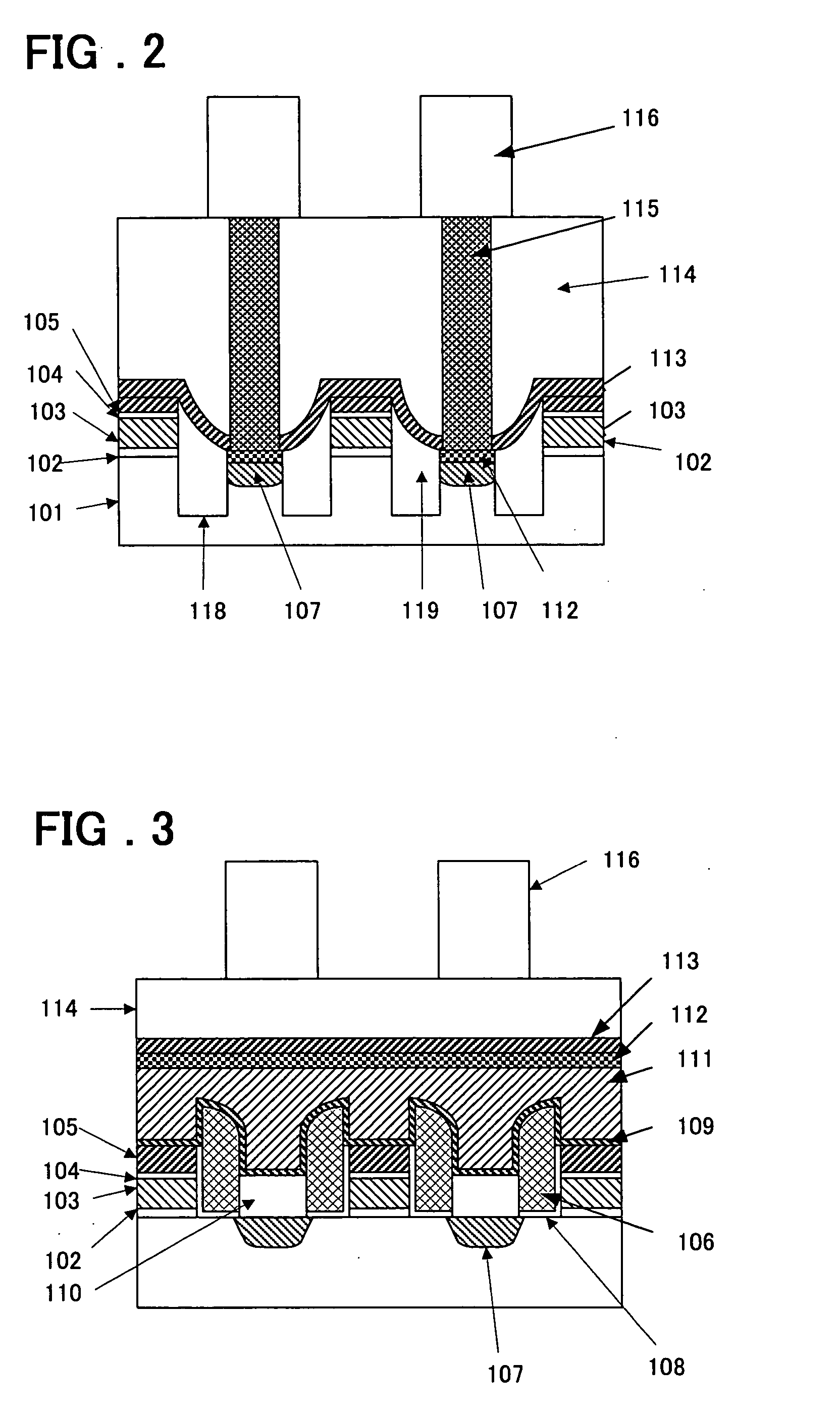
[0021] An embodiment of the present invention will now be described in detail with reference to the drawings.
[0022] A semiconductor storage device according to the present invention comprises a plurality of first-conductivity-type diffusion regions (107 in FIG. 1), each of which constitutes a bit line, extending in parallel with one another along one direction on the surface of a second-conductivity-type diffusion region that constitutes a memory cell area, and a select gate (103 in FIG. 1), which extends along the one direction and is disposed on a substrate, in a gap between two mutually adjacent ones of the first-conductivity-type diffusion regions. At the intersection of a word line (111 in FIG. 1) and the select gate, floating gates (106 in FIG. 1) are provided on the substrate via an insulating film on both sides of side walls of the select gate. The plurality of first-conductivity-type diffusion regions are connected from prescribed areas thereof to upper-layer interconnect ...
PUM
 Abstract
Description
Claims
Application Information