Methods for forming a barrier layer with periodic concentrations of elements and structures resulting therefrom

a technology of barrier layer and periodic concentration, applied in the field of processing a microelectronic topography, can solve the problems of affecting the fabrication specifications of film depositing, affecting the uniformity of thickness, and affecting the quality of the final produ

Inactive Publication Date: 2006-02-09
LAM RES CORP
View PDF34 Cites 26 Cited by
  • Summary
  • Abstract
  • Description
  • Claims
  • Application Information

AI Technical Summary

Benefits of technology

[0012] An embodiment of another of the methods includes forming a bulk metallic film upon the microelectronic topography using an electroless plating process. The bulk metallic film includes a bottom portion, a top portion, and an intermediate portion interposed between the bottom and top portions. One of the top and bottom portions includes a higher concentration of a first element than the intermediate portion and the other of the top and bottom portions. The method further includes annealing the microelectronic topography to induce diffusion of the first element within the bulk metallic film such that the intermediate portion comprises a higher concentration of the first element than the bottom and top portions.
[0013] An embodiment of yet another of the methods includes exposing a microelectronic topography to a deposition solution and forming a first sub-film portion by interfacial electroless reduction of a first element within the deposition solution until a second different element reaches a certain concentration within the deposition solution. The first sub-film includes a higher concentration of the first element than the second element. The method further includes forming a second sub-film portion upon and in contact with the first sub-film portion by chemical adsorption until

Problems solved by technology

In cases in which a film is electrolessly deposited across a microelectronic topography, however, obtaining thickness uniformity may be difficult.
In particular, some electroless plating techniques are susceptible to the “edge effect” in which portions of a film deposited near the edge of the wafer are thinner than the portions of the film deposited near the center of the wafer.
Such an effect also hinders fabrication specifications for depositing films having greater thicknesses near the edge

Method used


Image

  • Methods for forming a barrier layer with periodic concentrations of elements and structures resulting therefrom
  • Methods for forming a barrier layer with periodic concentrations of elements and structures resulting therefrom
  • Methods for forming a barrier layer with periodic concentrations of elements and structures resulting therefrom

Examples


Embodiment Construction

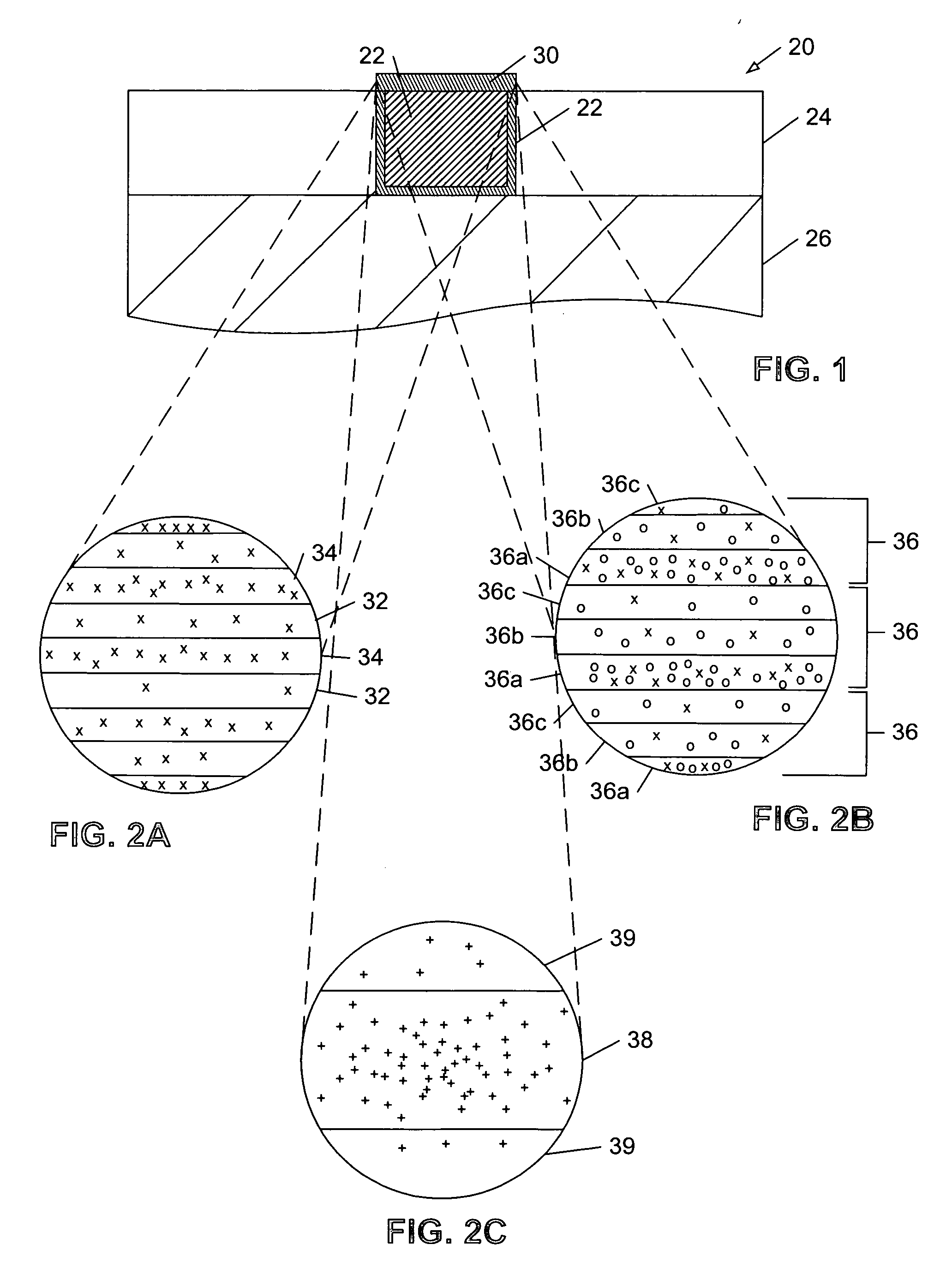
[0038] Turning to the drawings, exemplary methods and systems involving electroless plating processes for the formation of metallic layers and structures within microelectronic topographies are shown. In addition, microelectronic topographies resulting from the use of such methods and systems are shown. For instance, FIG. 1 illustrates a partial cross-sectional view of microelectronic topography 20 having liner layer 28, cap layer 30, as well as other metallic structures which may be formed from the methods and systems described below in reference to FIGS. 3-13. Although the methods and systems described below are specifically discussed in reference to the formation of barrier layers and, therefore, are specific to liner layer 28 and cap layer 30, any of the metallic structures of microelectronic topography 20, including those formed below lower layer 26 and those formed above cap layer 30, may be formed by the methods and systems described below in reference to FIGS. 3-13.

[0039] A...


PUM

PropertyMeasurementUnit
Fractionaaaaaaaaaa
Fractionaaaaaaaaaa
Fractionaaaaaaaaaa

Abstract

A method is provided which includes dispensing and removing different deposition solutions during an electroless deposition process to form different sub-films of a composite layer. Another method includes forming a film by an electroless deposition process and subsequently annealing the microelectronic topography to induce diffusion of an element within the film. Yet another method includes reiterating different mechanisms of deposition growth, namely interfacial electroless reduction and chemical adsorption, from a single deposition solution to form different sub-films of a composite layer. A microelectronic topography resulting from one or more of the methods includes a film formed in contact with a structure having a bulk concentration of a first element. The film has periodic successions of regions each comprising a region with a concentration of a second element greater than a set amount and a region with a concentration of the second element less than the set amount.

Description

PRIORITY APPLICATION [0001] The present application claims priority to provisional application no. 60 / 599,975 entitled “Methods and Systems for Processing a Microelectronic Topography” filed Aug. 9, 2004.BACKGROUND OF THE INVENTION [0002] 1. Field of the Invention [0003] This invention generally relates to methods for processing a microelectronic topography and more particularly to electroless plating processes performed upon microelectronic topographies and structures resulting therefrom. [0004] 2. Description of the Related Art [0005] The following descriptions and examples are not admitted to be prior art by virtue of their inclusion within this section. [0006] Electroless plating (also referred to herein as “electroless deposition”) is a process for depositing materials on a catalytic surface from an electrolyte solution without an external source of current. An advantage of an electroless plating process is that it can be selective, i.e., the material can be deposited only onto...

Claims


Application Information

Patent Timeline
IPC IPC(8): B05D1/18B22D7/00B22D25/00
CPCB82Y30/00Y10T428/24612C23C18/1651C23C18/1682C23C18/1683C25D5/08C25D7/12C25D21/10H01L21/288H01L21/6715H01L21/76801H01L21/76826H01L21/76829H01L21/76834H01L21/76843H01L21/76846H01L21/76849H01L21/76858H01L21/76864H01L21/76867H01L21/76877H01L23/53238C25D17/001Y10T428/12Y10T428/12458Y10T428/24479C23C18/1619H01L2924/0002H01L2924/00H01L21/76841
Inventor IVANOV, IGOR C.
Owner LAM RES CORP
Why Eureka
Try Eureka