Impedance conversion circuit, drive circuit, and control method therefor

a technology of impedance conversion and control method, which is applied in the direction of differential amplifiers, static indicating devices, instruments, etc., can solve the problems of power consumption, multi-colored images or movies are difficult to be displayed low power consumption is difficult to achieve on the other hand, so as to reduce the number of gray scale voltages to be generated, and reduce the number of gray scale voltage signal lines supplied with the generated gray scale voltag

Inactive Publication Date: 2006-02-16
SEIKO EPSON CORP
View PDF10 Cites 8 Cited by
  • Summary
  • Abstract
  • Description
  • Claims
  • Application Information

AI Technical Summary

Benefits of technology

[0016] In view of the problems, an aspect of the invention relates to an impedance conversion circuit for outputting a voltage corresponding to (j+k) (j, k: positive integers) bits of gray scale data, including an input for receiving an input voltage selected from 2j levels of voltages in accordance with high j bit(s) of the gray scale data, and an output for outputting an output voltage corresponding to low k bit(s) of the gray scale data from 2k levels of voltages obtained by changing a potential of the input voltage.
[0017] In this aspect of the invention, either of the 2j levels of voltage corresponding to the high j bits data of (j+k) bits gray scale data is received as the input voltage, and the impedance conversion circuit outputs the voltage corresponding to low k bits of the gray scale data from the 2k levels of voltages based on the input voltage. Therefore, it is enough to select the input voltage from the 2j levels of gray scale voltages. Thus, since the number of gray scale voltage signal lines can be reduced while maintaining the number of gray scale levels, the number of gray scale voltages to be generated can be reduced. And, the number of gray scale voltage signal lines supplied with the generated gray scale voltages can be reduced, thus making the width of the wiring region narrower. As a result, the ratio of the area the wiring region for the gray scale voltage signal lines occupies can be held in a low level. Thus, even with an increased number of gray scale levels, the chip area of the data driver implementing the impedance conversion circuit can be reduced to achieve cost reduction.
[0018] Further, in an impedance conversion circuit according to another aspect the invention, an operational amplifier connected to form a voltage follower and having an input supplied with the input voltage, and an output voltage setting circuit for pre-charging or discharging an output of the operational amplifier in accordance with the least significant bit data of the gray scale data can also be included. The operational amplifier outputs the output voltage different from the input voltage by a dead zone width of the operational amplifier after the output voltage setting circuit pre-charges or discharges the output of the operational amplifier.
[0019] Further, in the impedance conversion circuit according to another aspect of the invention, the source of each transistor is supplied with a current from the first current source. The operational amplifier can include a first differential amplifier circuit of a first conductivity type having a first differential transistor pair of the first conductivity type and a first current mirror circuit, a second differential amplifier circuit of a second conductivity type having a second differential transistor pair of the second conductivity type and a second current mirror circuit, and an output circuit having a first drive transistor of the second conductivity type and a second drive transistor of the first conductivity type.
[0020] The gate of the each of the first differential transistor pair of the first conductivity type is respectively supplied with the input voltage and the output voltage. The first current mirror circuit generates a drain current for each transistor of the first differential transistor pair. The source of each of the transistors of the second differential transistor pair of the second conductivity type is supplied with a current from the second current source, and the gate of each of the transistors is respectively supplied with the input voltage and the output voltage. The second current mirror circuit generates a drain current for each transistor of the second differential transistor pair.
[0021] The gate voltage of the first drive transistor of the second conductivity type is controlled in accordance with the drain voltage of the input side of the transistors forming the first differential transistor pair. The gate of the input side of the transistors is supplied with the input voltage. Further, the gate voltage of the second drive transistor of the first conductivity type is controlled in accordance with the drain voltage of the input side of the transistors forming the second differential transistor pair. The gate of the input side of the transistors is supplied with the input voltage. The output circuit outputs a voltage of the node through which the drains of the first and the second drive transistors are connected to each other. A current drive efficiency of the input side of the first pair of transistors is arranged to be lower than a current drive efficiency of the other, namely the output side of the first pair of transistors. A current drive efficiency of the input side of the second pair of transistors is arranged to be lower than a current drive efficiency of the other, namely the output side of the second pair of transistors.

Problems solved by technology

The simple matrix method has an advantage that low power consumption can more easily be achieved compared to the active matrix method on the one hand, and has a disadvantage that multi-colored images or movies are difficult to be displayed on the other hand.
In contrast, the active matrix method has an advantage that it is suitable for displaying multi-colored images or movies on the one hand, and has a disadvantage that low power consumption is difficult to be achieved on the other hand.
Therefore, the ratio at which the wiring region for the group of gray scale voltage signals occupies becomes larger and larger as the multi-gray scale display enhances, thus causing high manufacturing cost due to the enlarged area for layout.

Method used


Image

  • Impedance conversion circuit, drive circuit, and control method therefor
  • Impedance conversion circuit, drive circuit, and control method therefor
  • Impedance conversion circuit, drive circuit, and control method therefor

Examples


Embodiment Construction

[0062] Hereinafter, an embodiment of the invention is described in detail with reference to the accompanying drawings. Note that the embodiment described below does not unreasonably limit the content of the invention as claimed in the claim section. Further, not all of the components of the configuration described below are essential elements of the invention.

[0063] 1. Liquid Crystal Device

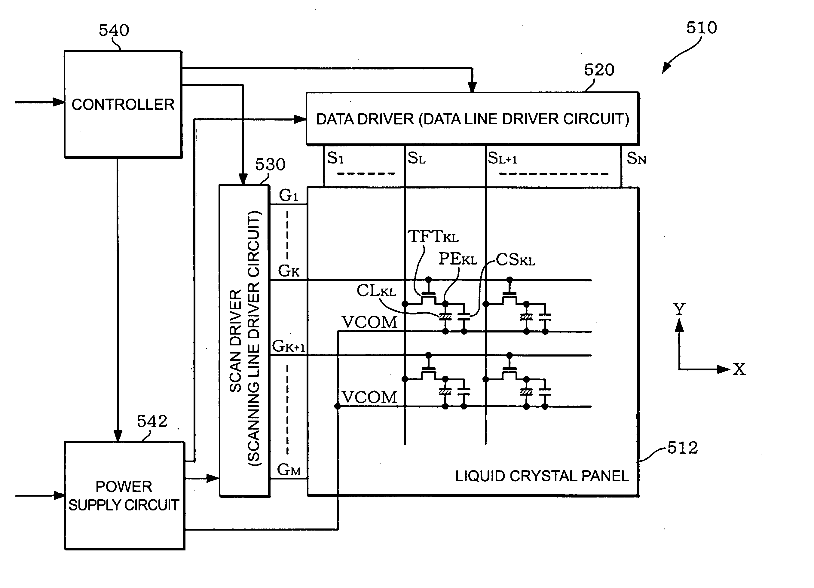
[0064]FIG. 1 shows an example of a block diagram of a liquid crystal device implementing an impedance conversion circuit according to the present embodiment.

[0065] The liquid crystal device (a display device, in a broad sense) 510 includes a liquid crystal panel (a display panel, in a broad sense) 512, a data driver (a data line driver circuit) 520, a scan driver (a scanning line driver circuit) 530, a controller 540, and a power source circuit 542. Note that the liquid crystal device does not necessarily include all of these circuit blocks, but a configuration without a part of these circuit b...


PUM


Abstract

An impedance conversion circuit for outputting a voltage corresponding to (j+K) (j, k: positive integers) bits of gray scale data, including: an input for receiving an input voltage selected from 2j levels of voltages in accordance with high j bit(s) of the gray scale data; and an output for outputting an output voltage corresponding to low k bit(s) of the gray scale data from 2k levels of voltages obtained by changing a potential of the input voltage.

Description

BACKGROUND OF THE INVENTION [0001] 1. Technical Field [0002] The present invention relates to an impedance conversion circuit, a drive circuit, and a control method for the impedance circuit. [0003] 2. Related Art [0004] In the related art, as liquid crystal panels (electro-optic devices, in a broad sense) used for electronic apparatuses such as mobile phones, simple matrix liquid crystal panels and active matrix liquid crystal panels using switching elements such as thin film transistors (hereinafter abbreviated as TFT) are known. [0005] The simple matrix method has an advantage that low power consumption can more easily be achieved compared to the active matrix method on the one hand, and has a disadvantage that multi-colored images or movies are difficult to be displayed on the other hand. In contrast, the active matrix method has an advantage that it is suitable for displaying multi-colored images or movies on the one hand, and has a disadvantage that low power consumption is di...

Claims


Application Information

Patent Timeline
Patent Type & Authority Applications(United States)
IPC IPC(8): G09G3/36
CPCG09G2310/027G09G3/3688G09G3/36H03F3/45G09G3/20
Inventor MAKI, KATSUHIKO
Owner SEIKO EPSON CORP
Why Eureka
Try Eureka