

System and method to compensate for static and dynamic misalignments and deformations in a maskless lithography tool
a maskless lithography and tool technology, applied in the field of lithography, can solve the problems of dynamic displacement of slm arrays, spatial distortion of images, and deformation of printed patterns, and achieve the effects of reducing the accuracy of printed patterns
- Summary
- Abstract
- Description
- Claims
- Application Information
AI Technical Summary
Benefits of technology
Problems solved by technology
Method used
Image

Examples
Embodiment Construction
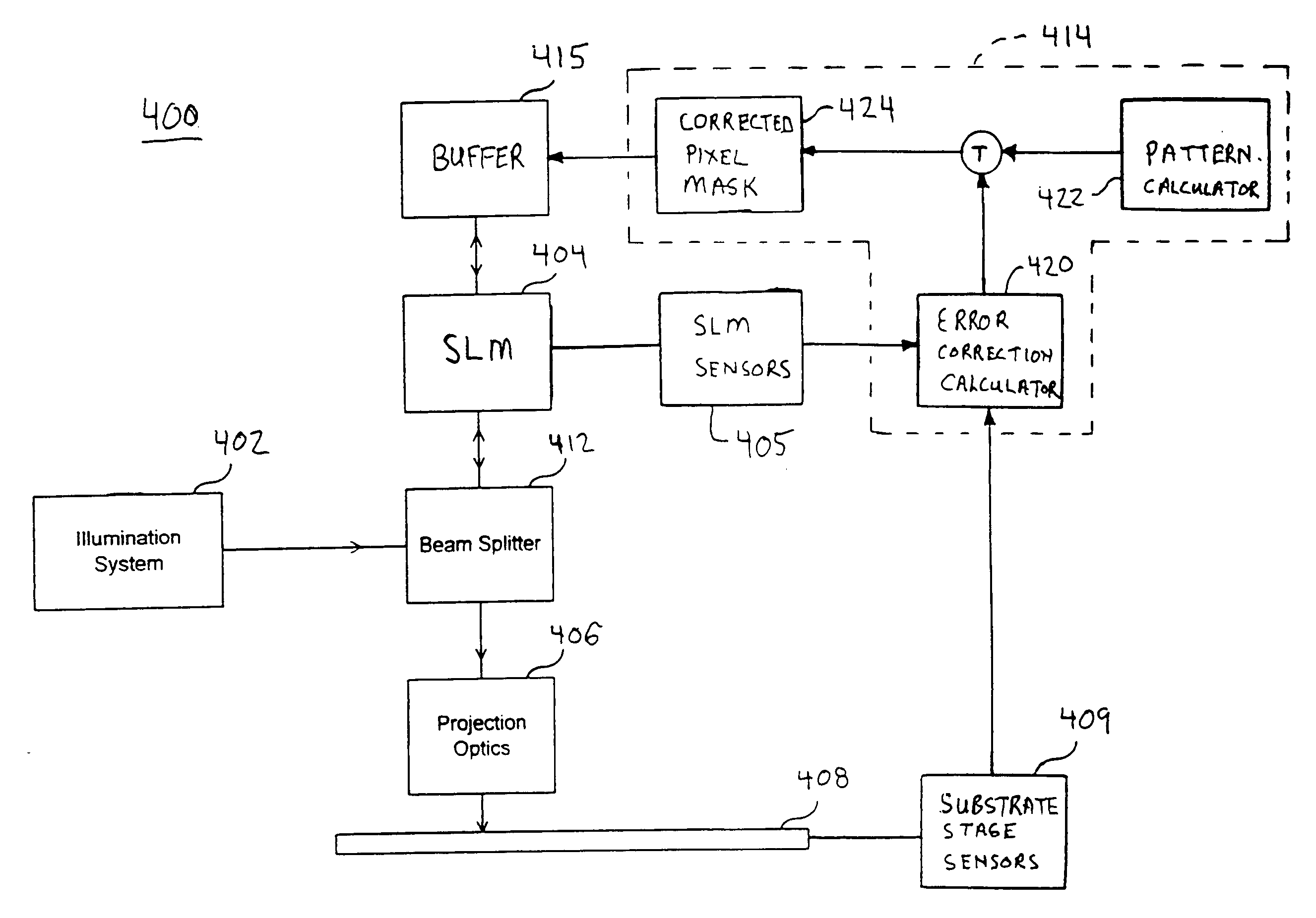
[0030] The present invention provides systems and methods for improved maskless lithographic printing that compensate for static and dynamic position misalignments and deformations. While specific configurations and arrangements are discussed, it should be understood that this is done for illustrative purposes only. Persons skilled in the art(s) will recognize that other configurations and arrangements can be used without departing from the spirit and scope of the present invention. It will be apparent to persons skilled in the pertinent art(s) that this invention can be employed in a variety of other applications.
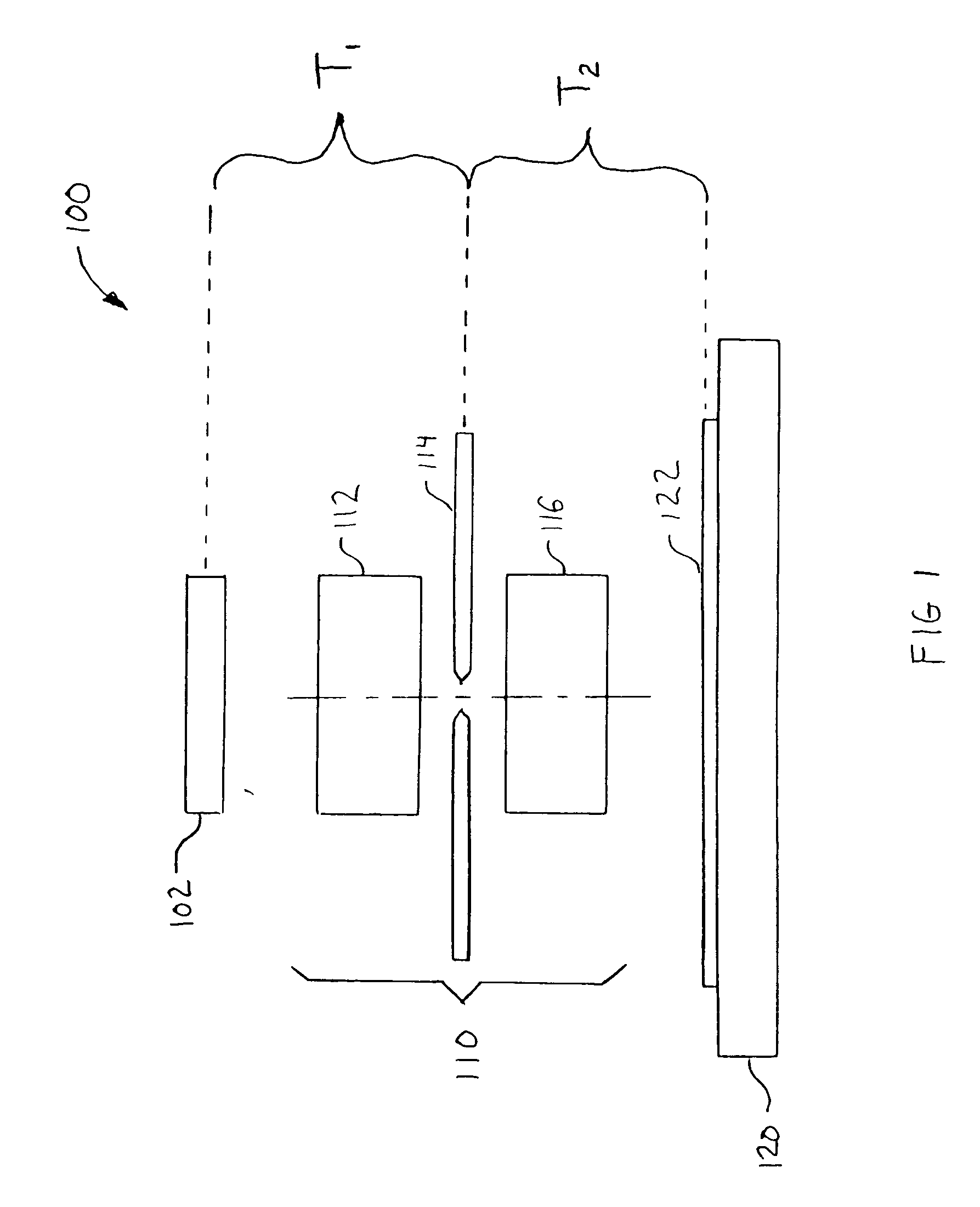
[0031]FIG. 1 is a schematic illustration of a maskless lithography system 100 in which the present invention is used. System 100 includes a spatial light modulator 102, projection optics 110, and a substrate stage 120. Projection optics 110 typically include optical elements 112, an aperture 114, and optical elements 116. An object 122 (e.g., wafer of substrate) to be exp...
PUM
 Abstract
Description
Claims
Application Information