Memory cell structure

a memory cell and cell structure technology, applied in the field of memory cell structure systems, can solve the problems of soft errors, small cmos devices, and large challenges,

Active Publication Date: 2006-02-23
TAIWAN SEMICON MFG CO LTD
View PDF11 Cites 155 Cited by
  • Summary
  • Abstract
  • Description
  • Claims
  • Application Information

AI Technical Summary

Benefits of technology

[0017] In accordance with still another aspect of the present invention, a semiconductor device is provided, which includes a substrate. An SRAM device is in the substrate, and a memory cell is in the SRAM device. The memory cell includes an NWELL region and a PWELL region. The memory cell also includes a cell area. The cell area includes a first cell pitch aligned along a latitudinal...

Problems solved by technology

Significant challenges, however, are faced as the sizes of CMOS devices continue to decrease.
One such challenge is soft errors.
Soft errors are errors that occur in the logic state of a circuit due to excess charge carriers, which are typically induced by alpha-particles and cosmic ray neutrons.
Soft errors occurring in SRA...

Method used


Image

  • Memory cell structure
  • Memory cell structure
  • Memory cell structure

Examples


first embodiment

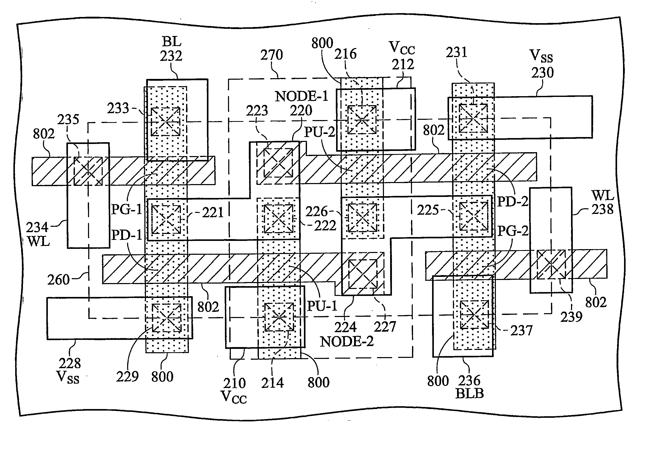
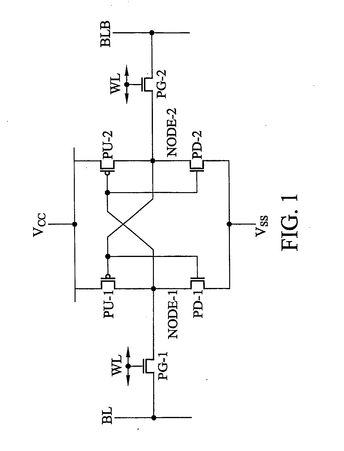
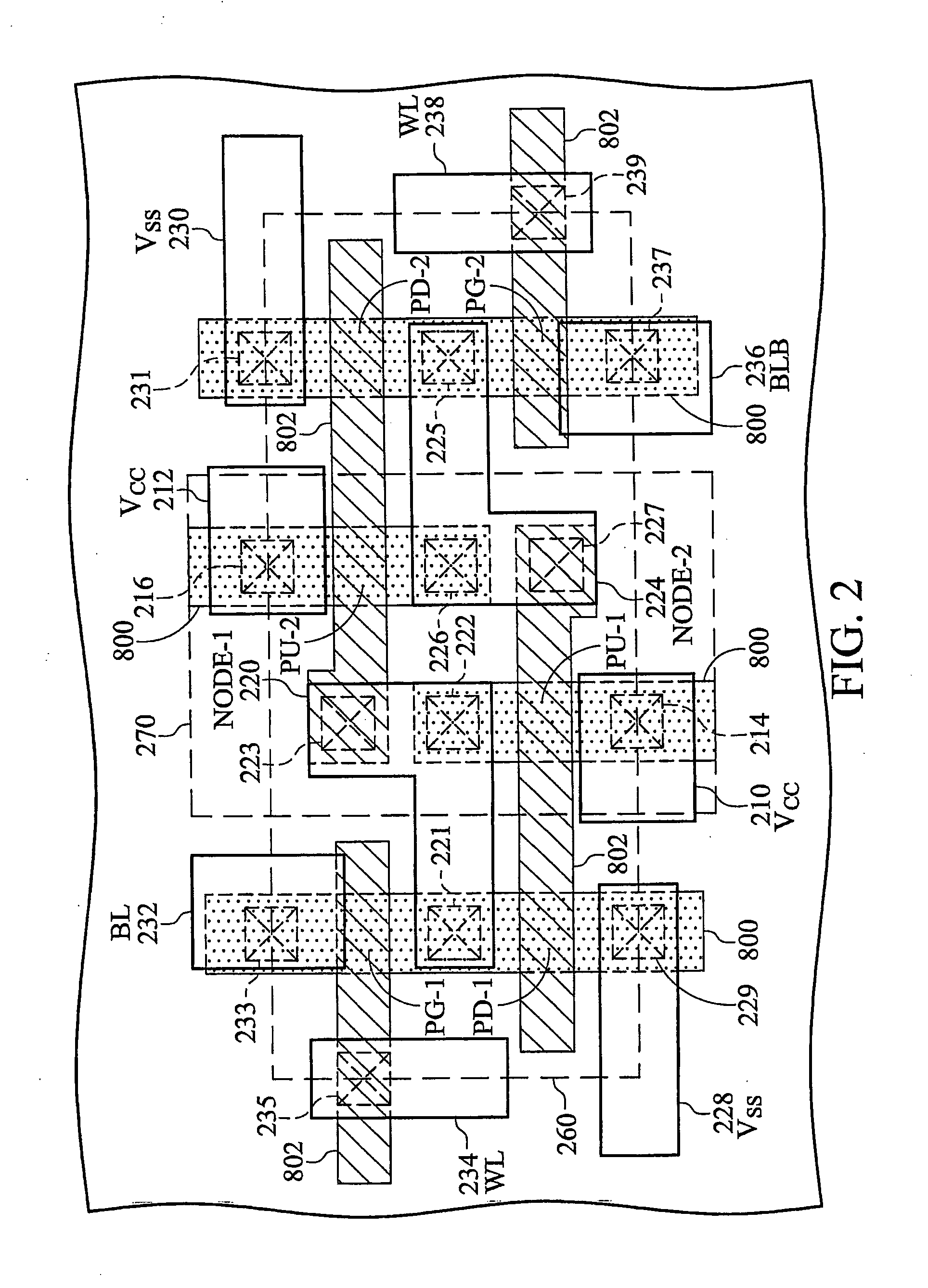
[0034] Referring first to FIG. 1, a schematic diagram of the 6T-SRAM cell of the first embodiment is shown. Generally, the 6T-SRAM cell comprises a first pass-gate transistor PG-1, a second pass-gate transistor PG-2, a first pull-up transistor PU-1, a second pull-up transistor PU-2, a first pull-down transistor PD-1, and a second pull-down transistor PD-2.

[0035] In operation, the memory cell of the first embodiment forms two complementary nodes, shown as NODE-1 and NODE-2 in FIG. 1. Because NODE-1 is tied to the gate of the second pull-up transistor PU-2 and NODE-2 is tied to the gate of the first pull-up transistor PU-1, the values stored in each node will remain complementary to each other. For example, when NODE-1 is high, the PMOS second pull-up transistor PU-2 prevents the current from the current source Vcc from flowing to NODE-2. In parallel, the gate of the NMOS second pull-down transistor PD-2 is activated, allowing any charge that may be in NODE-2 to go to ground. Furtherm...

third embodiment

[0060]FIGS. 5a and 5b show a 6T-SRAM cell in accordance with a third illustrative embodiment of the present invention. FIG. 5a shows a cross sectional view of the 6T-SRAM cell 500 of the The discussion of the third illustrative embodiment also includes FIG. 5b, which shows a plan view of the pull down transistor 508 in the third illustrative embodiment.

[0061]FIG. 5a shows an SRAM cell 500 of the third illustrative embodiment. The substrate 502 is preferably a bulk silicon substrate. Other substrates may be used, including silicon on insulator (SOI) substrates, substrates having a substantially crystalline structure with a Miller indices of , and substrates having a substantially crystalline structure with a Miller indices of , for example.

[0062] An n-type metal oxide semiconductor (NMOS) transistor 504 of the third embodiment is shown in FIG. 5a in a PWELL region 506. The NMOS transistor 504 is shown beside a p-type metal oxide semiconductor (PMOS) transistor 508 in an NWELL regio...

fifth embodiment

[0073]FIGS. 8 and 9 show a 6T-SRAM cell in accordance with a fifth illustrative embodiment of the present invention. FIG. 8 is a schematic view of a dual port 8T-SRAM cell 660 of the FIG. 9 is a cell layout of the dual port 8T-SRAM cell 660 of the fifth illustrative embodiment.

[0074] In accordance with a fifth illustrative embodiment, a dual port eight transistor (8T) SRAM cell 660 is shown in FIG. 8. In operation, the 8T-SRAM 660 operates substantially the same as a 6T-SRAM. In contrast with a 6T-SRAM however, the dual port 8T SRAM cell 660 of the fifth embodiment includes two ports, PORT-A and PORT-B. PORT-A includes the NMOS pass gate transistor PG-1, the NMOS pass gate transistor PG-2, the bit line BLA, the complementary bit line BLB, and the word line WL-A. PORT-B includes the NMOS pass gate transistor PG-3, the NMOS pass gate transistor PG-4, the bit line BLB, the complementary bit line BLBB, and the word line WL-B. The two bit lines, i.e., bit line A (BLA) and bit line B (BL...


PUM


Abstract

An SRAM device includes an SRAM cell in a deep NWELL region in a substrate. PWELL regions in the SRAM cell occupy less than about 65% of the cell area of the SRAM cell. A ratio of a longer side of a cell area of the SRAM cell to a shorter side of the SRAM cell is larger than about 1.8. A total area of the active regions in the plurality of NMOS transistors in the SRAM cell occupies less than about 25% of the SRAM cell area. A ratio of the channel width of a pull up transistor in the SRAM cell to the channel width of a pull down transistor in the SRAM cell is greater than about 0.8. The SRAM cell further includes a boron free inter-layer-dielectric layer, an inter-metal-dielectric layer with dielectric constant less than about 3, and a polyimide layer with a thickness of less than about 20 microns.

Description

[0001] This application claims the benefit of U.S. Provisional Application No. 60 / 603,695, filed on Aug. 23, 2004, entitled Memory Cell Structure, which application is hereby incorporated herein by reference.TECHNICAL FIELD [0002] The present invention relates generally to semiconductor devices and more particularly to a system for a memory cell structure. BACKGROUND [0003] Complementary metal-oxide-semiconductor (CMOS) technology is the dominant semiconductor technology used for the manufacture of ultra-large scale integrated (ULSI) circuits today. Size reduction of the semiconductor structures has provided significant improvement in the speed, performance, circuit density, and cost per unit function of semiconductor chips over the past few decades. Significant challenges, however, are faced as the sizes of CMOS devices continue to decrease. [0004] One such challenge is soft errors. Soft errors are errors that occur in the logic state of a circuit due to excess charge carriers, whi...

Claims


Application Information

Patent Timeline
IPC IPC(8): H01L29/94
CPCG11C8/16H01L27/1104H01L27/11G11C11/412H10B10/00H10B10/12
Inventor LIAW, JHON-JHY
Owner TAIWAN SEMICON MFG CO LTD
Why Eureka
Try Eureka