
Semiconductor chip manufacturing method, semiconductor chip, semiconductor device manufacturing method, and semiconductor device

a semiconductor chip and manufacturing method technology, applied in the direction of semiconductor devices, semiconductor/solid-state device details, electrical devices, etc., can solve the problem of deteriorating the properties of the semiconductor chip

Active Publication Date: 2006-02-23
KIOXIA CORP +2
View PDF3 Cites 51 Cited by
  • Summary
  • Abstract
  • Description
  • Claims
  • Application Information

AI Technical Summary

Benefits of technology

[0072] The aforementioned objects, other objects, features, and advantageous effects of the present invention will become apparent from the following description of embodiments given with reference to the accompanying drawings.

Problems solved by technology

Thus, the wafer W is contaminated, and the properties of the semiconductor chip are deteriorated.

Method used


Image

  • Semiconductor chip manufacturing method, semiconductor chip, semiconductor device manufacturing method, and semiconductor device
  • Semiconductor chip manufacturing method, semiconductor chip, semiconductor device manufacturing method, and semiconductor device
  • Semiconductor chip manufacturing method, semiconductor chip, semiconductor device manufacturing method, and semiconductor device

Examples


first embodiment

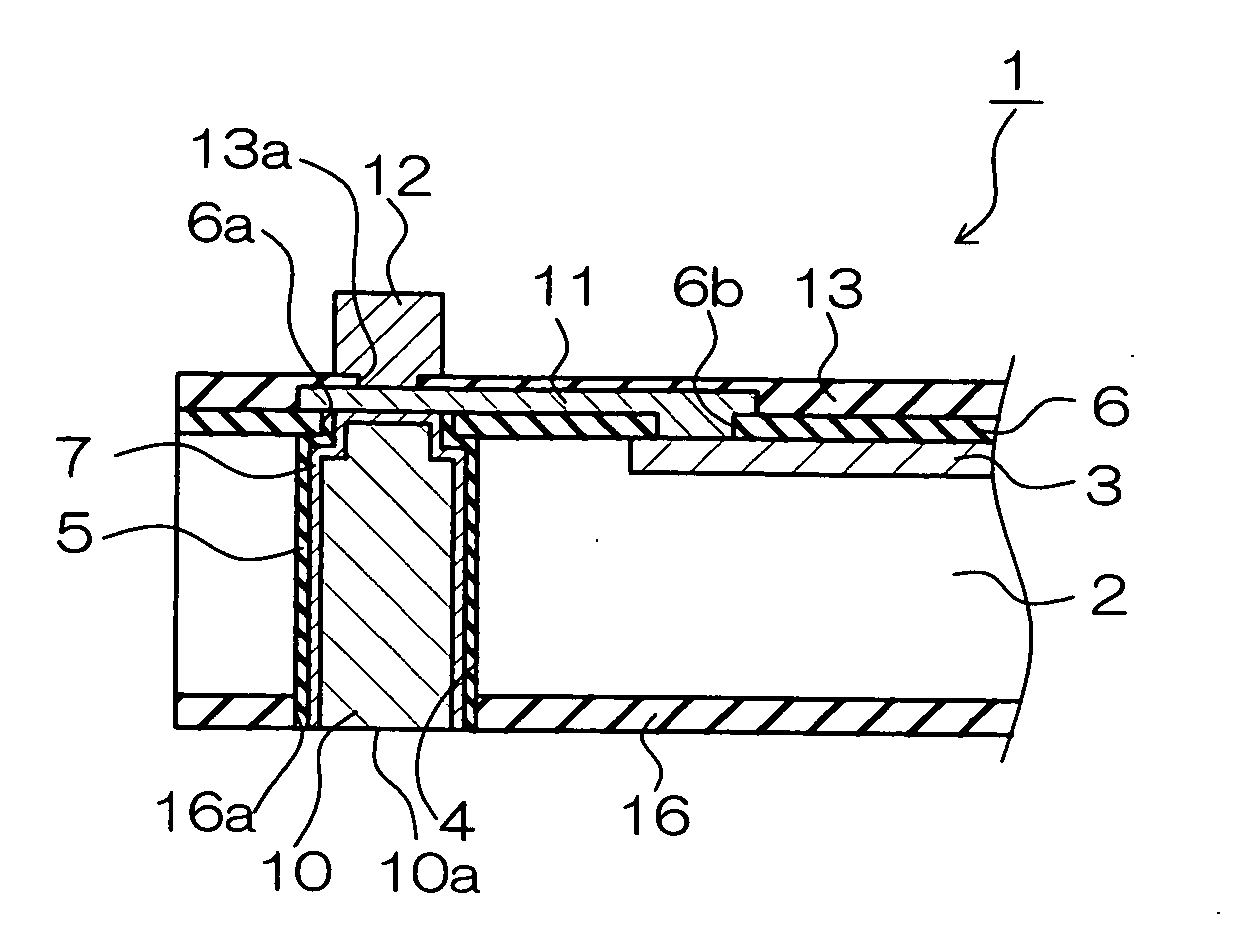
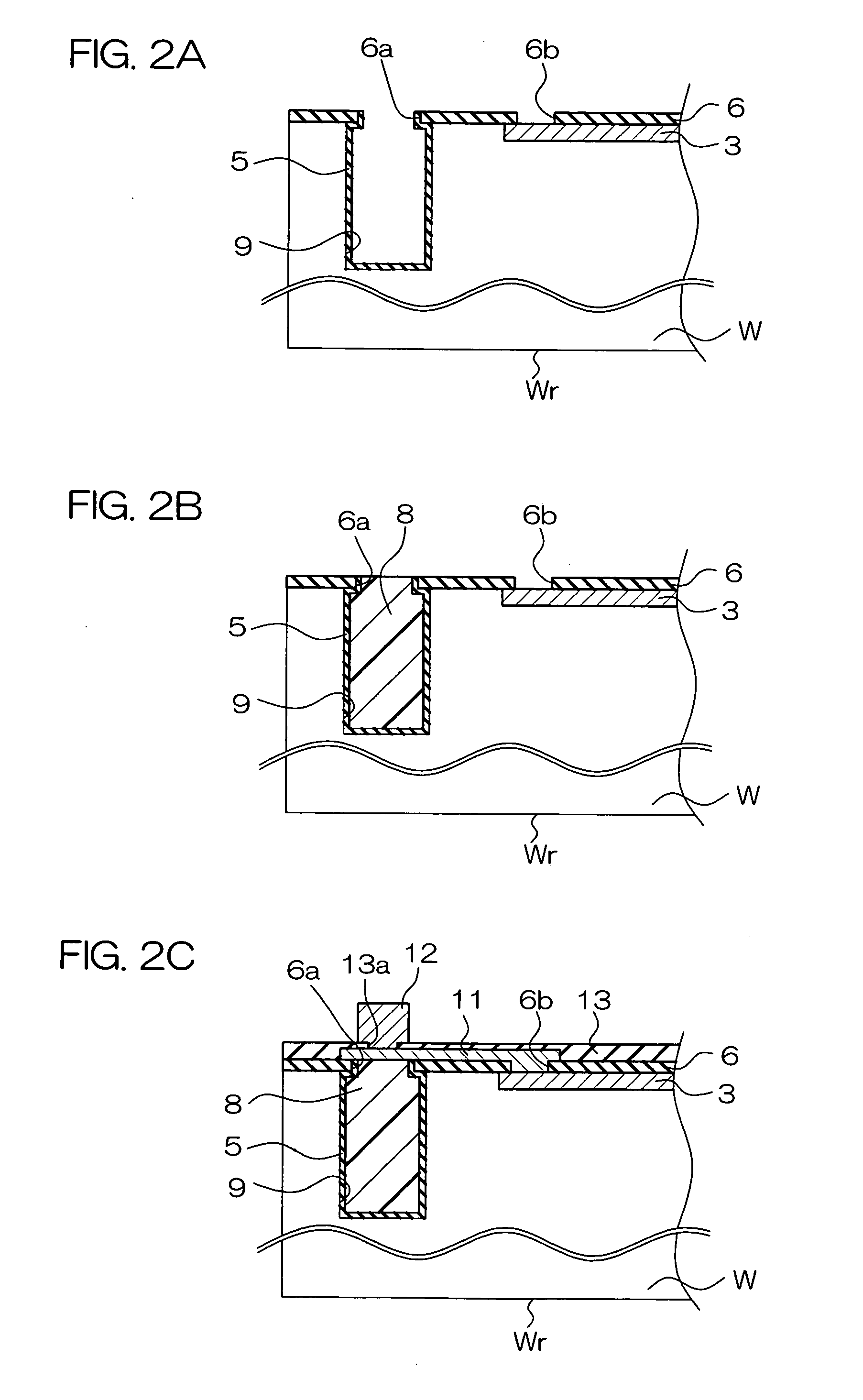
[0087]FIG. 1 is a diagrammatic sectional view showing a structure of a semiconductor chip produced by a manufacturing method according to the present invention.

[0088] This semiconductor chip 1 includes a semiconductor substrate 2 made of silicon, for example. A functional device (an active element such as a transistor or a passive element such as a resistor or a capacitor) 3 that has a plurality of electrodes is formed on one surface (hereinafter, referred to as “front surface”) of the semiconductor substrate 2. A through-hole 4 that penetrates the semiconductor substrate 2 in a thickness direction is formed beside the functional device 3.

[0089] A hard mask 6 made of, for example, silicon oxide is formed on the front surface of the semiconductor substrate 2. The hard mask 6 has an opening 6a and a contact hole 6b. The opening 6a is formed in a region where the opening 6a substantially coincides with the through-hole 4 when viewed perpendicularly to the front surface of the semicond...

second embodiment

[0118]FIG. 3 is a diagrammatic sectional view showing a structure of a semiconductor chip produced by a manufacturing method according to the present invention. In FIG. 3, the same reference symbol as in FIG. 1 is given to an element corresponding to each element of FIG. 1, and a description thereof is omitted.

[0119] This semiconductor chip 31 has a connection pattern 32 provided in a region around the through-hole 4 on the side of the rear surface of the semiconductor substrate 2. The connection pattern 32 is formed integrally with the penetration electrode 10, and is made of the same kind of material as the penetration electrode 10, i.e., is made of copper. A diffusion preventing film 7 is interposed between the connection pattern 32 and the rear-surface protecting film 16.

[0120] The surface of the connection pattern 32 serves as a rear-side connection surface 32a to obtain an electrical connection with the outside of the semiconductor chip 31. A bump of another semiconductor chi...

third embodiment

[0122]FIG. 4 is a diagrammatic sectional view showing a structure of a semiconductor chip produced by a manufacturing method according to the present invention. In FIG. 4, the same reference symbol as in FIG. 1 is given to an element corresponding to each element of FIG. 1, and a description thereof is omitted.

[0123] An insulating film 42 made of photosensitive resin, a diffusion preventing film 43, and a penetration electrode 45 made of copper are provided inside the through-hole 4 and the opening 6a of the semiconductor chip 41. The insulating film 42 is provided on the whole surface of the inner wall of the through-hole 4 and the opening 6a. The penetration electrode 45 is disposed along the center axis of the through-hole 4 in an inner region of the insulating film 42. The diffusion preventing film 43 is interposed between the insulating film 42 and the penetration electrode 45 and between the wiring member 11 and the penetration electrode 45.

[0124] The insulating film 42 is th...


PUM


Abstract

The invention provides a semiconductor chip manufacturing method, including a step of forming a front-surface-side concave portion in a semiconductor substrate having a front surface and a rear surface, a functional device being formed on the front surface, the front-surface-side concave portion being formed in the front surface and having a predetermined depth smaller than a thickness of the semiconductor substrate; a dummy plug forming step of supplying nonmetallic material into the front-surface-side concave portion and embedding a dummy plug made of the nonmetallic material; a thinning step of removing a part of the rear surface of the substrate and thinning the semiconductor substrate so that the thickness of the semiconductor substrate becomes smaller than the depth of the front-surface-side concave portion and so that the front-surface-side concave portion is formed into a through-hole; a dummy plug removing step of removing the dummy plug; and a step of supplying metallic material into the through-hole and forming a penetration electrode.

Description

BACKGROUND OF THE INVENTION [0001] 1. Field of the Invention [0002] This invention relates to a semiconductor chip that has a through-hole penetrating in its thickness direction, a method for manufacturing the semiconductor chip, a semiconductor device that has a semiconductor chip having a through-hole penetrating in its thickness direction, and a method for manufacturing the semiconductor device. [0003] 2. Description of Related Art [0004] A multichip module (MCM) is known as a semiconductor device having a plurality of semiconductor chips. In the multichip module, an attempt has been made to reduce the mounting area of a semiconductor device by stacking a plurality of semiconductor chips together on a wiring substrate in the semiconductor device. In some of the thus structured semiconductor devices, a penetration electrode is provided in a through-hole penetrating through semiconductor chips in the thickness direction, and a longitudinal electrical connection is achieved by this ...

Claims


Application Information

Patent Timeline
IPC IPC(8): H01L23/48
CPCH01L21/76898H01L2224/0401H01L24/16H01L25/0657H01L25/50H01L2224/05009H01L2224/13009H01L2224/13025H01L2224/13099H01L2224/48091H01L2224/48227H01L2225/0651H01L2225/06513H01L2225/06524H01L2225/06541H01L2225/06586H01L2924/01013H01L2924/01022H01L2924/01029H01L2924/01033H01L2924/01049H01L2924/01057H01L2924/01058H01L2924/01061H01L2924/01073H01L2924/01074H01L2924/01075H01L2924/01078H01L2924/01079H01L2924/01082H01L2924/04941H01L2924/04953H01L2924/14H01L2924/15311H01L2924/19041H01L2924/3025H01L23/481H01L2224/73204H01L2224/32145H01L2224/16145H01L2924/12041H01L2924/014H01L2924/01068H01L2924/01024H01L2924/01006H01L2924/01005H01L24/48H01L2224/9202H01L2924/00014H01L2924/00H01L2924/00012H01L2924/181H01L2924/00011H01L2224/023H01L2224/45099H01L2224/45015H01L2924/207H01L2924/01032H01L2924/0001H01L23/12H01L21/76831
Inventor TANIDA, KAZUMASANEMOTO, YOSHIHIKOTAKAHASHI, KENJI
Owner KIOXIA CORP
Features
  • Generate Ideas
  • Intellectual Property
  • Life Sciences
  • Materials
  • Tech Scout
  • Unparalleled Data Quality
  • Higher Quality Content
  • 60% Fewer Hallucinations
Learn More