Thermally Tunable Laser with Single Solid Etalon Wavelength Locker

Inactive Publication Date: 2006-02-23
HUANG RONG
18 Cites 21 Cited by

AI-Extracted Technical Summary

Problems solved by technology

The air-spaced etalon is bulky and expensive.
It is not compatible with an industry trend...

Benefits of technology

[0009] And yet another object of the present invention is to provide for reduced assem...

Abstract

A thermally tunable semiconductor laser and a wavelength locker are integrated on one single platform. The temperature of the platform, and the semiconductor, and the wavelength locker is actively adjusted by a thermal electrical cooler. The etalon has a free space range of material dispersion compensated according to the refractive index dependence on the wavelength of the etalon and temperature compensated according to the wavelength dependence of the temperature of the semiconductor laser. The locking point value is adjusted during the operation according to the measured temperature of the etalon.

Application Domain

Technology Topic

Tunable laserSemiconductor laser theory +3

Image

  • Thermally Tunable Laser with Single Solid Etalon Wavelength Locker
  • Thermally Tunable Laser with Single Solid Etalon Wavelength Locker
  • Thermally Tunable Laser with Single Solid Etalon Wavelength Locker

Examples

  • Experimental program(1)

Example

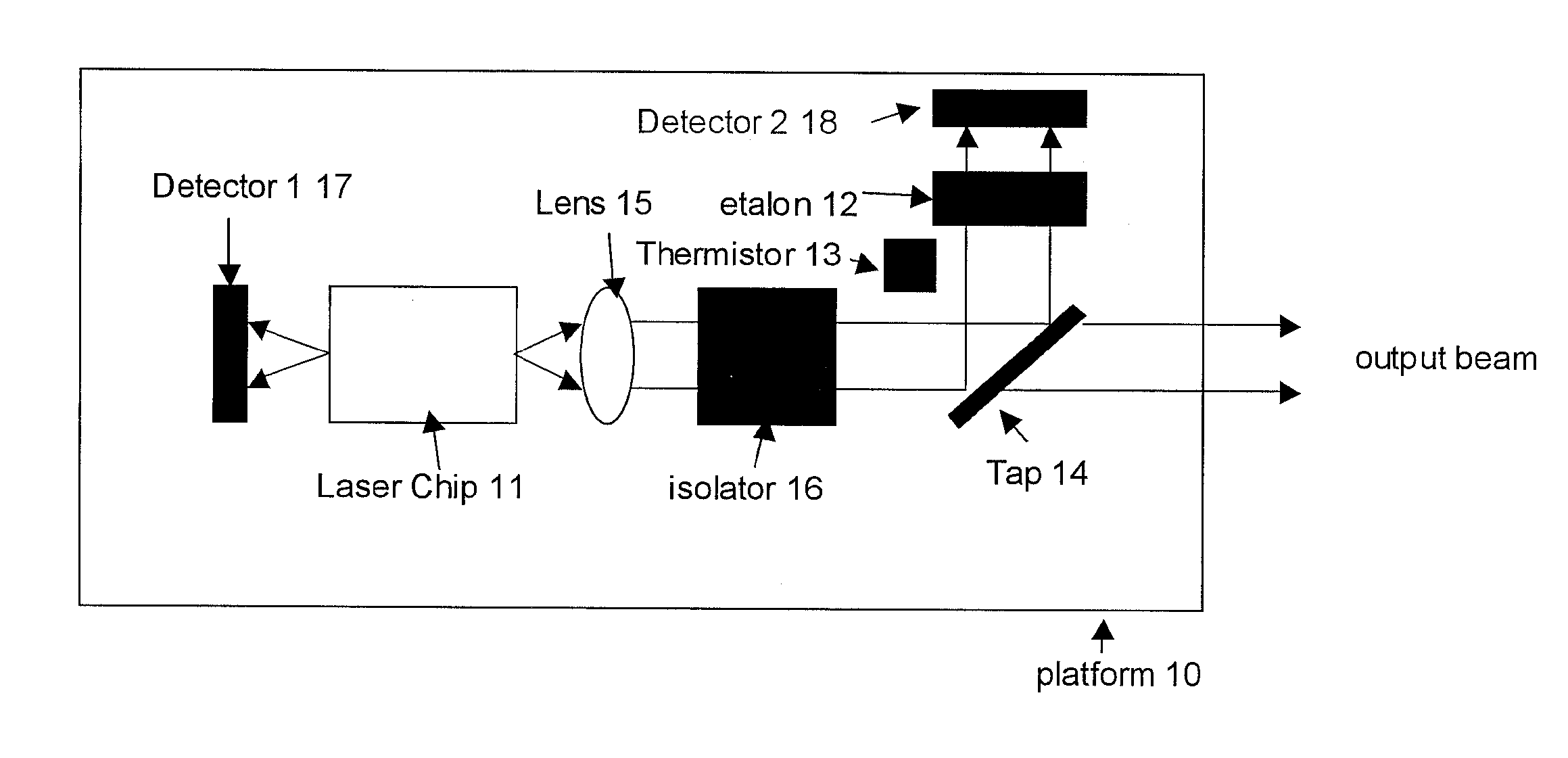
[0017] Distributed feedback semiconductor lasers or distributed Bragg reflection semiconductor lasers are a key device and widely deployed in optical communication. their wavelength can be thermally tuned for a few 100 GHz. To meet the strict requirement of the wavelength stability, their wavelength is controlled by a wavelength locker, in which usually a Fabry-Perot etalon is used as a wavelength discriminator.
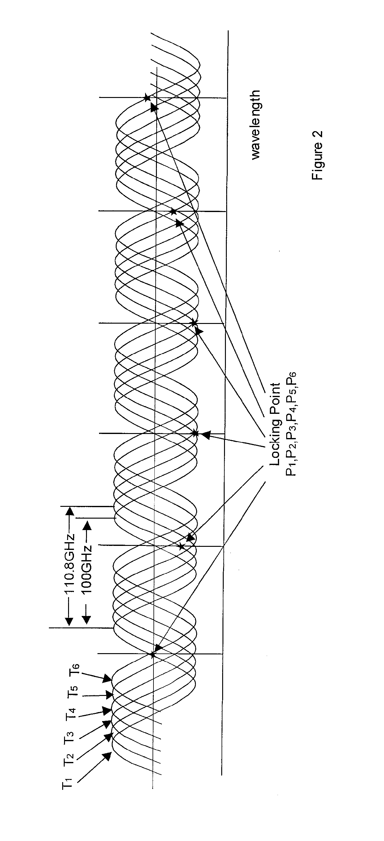
[0018] The etalon in a wavelength locker usually has 100 GHz free spectrum range, which is equal to the most popular ITU-defined channel spacing. When it is used to lock a thermally tunable laser, the temperature dependence of the FSR of the etalon becomes a concern. If a solid etalon is made of, e.g., fused silica, the etalon is placed on a separate temperature controller from the laser diode; other-wise, an air-spaced etalon is used to counter the temperature fluctuation. Either ways increase packaging complicacy and the cost. The laser diode and etalon co-packaged on one platform is preferred.
[0019] One of wavelength locker and laser diode arrangements is shown in the FIG. 1 for example. The wavelength locker and the laser diode are packaged on single platform, which is made of a highly thermally conductive material, such as AIN and Kovar. There are various ways to layout the laser diode and the wavelength locker on the platform as described in prior arts. The output wavelength from the laser diode is adjusted by changing the temperature of the laser diode, for example, by sitting the platform on a thermal electrical cooler. The detector 117 sits behinds the laser diode to monitor the power output. The output beam is collimated from its front side, and passes through a isolator 17. A tap 14 sits an angle in the path of the beam to deviate a small portion of the beam towards the etalon, which sits intentionally perpendicular to the incoming optical beam. The second detector 18 is set behind the etalon to record the wavelength-dependent intensity. The ratio of the signal from the detector 218 to the detector 117 tells the output wavelength of the laser diode. Comparing to a pre-calibrated ratio (for a channel wavelength at a calibration temperature T), the diode is set to the channel wavelength.
[0020] If the temperature of the platform changes, the transmission fringes of the etalon shift. As shown in FIG. 2, the transmission fringes of an etalon with FSR 100 GHz shift left further and further with the increase of the temperature for such as fused silica etalon. For example, at the temperature T1, T2, T3, T4, T5, T6, the output wavelengths from the laser diode are channel 1, 2, 3, 4, 5 and 6 and the locking points on the flanks of the transmission fringes are P1, P2, P3, P4, P5, and P6, respectively. Initially, at the temperature T1, the locking point P1 is set at the middle of one flank of the transmission fringes with a maximum slope which allows the most accurate wave-length locking subject to a given intensity detection accuracy. The locking points P2, P3, P4, P5, and P6 are around the middle of their respective flank. However, at the temperature T2, the locking point P2 slips down the flank, as shown in the FIG. 2. At the temperature T3 and T4, the locking points slip further to the valley of the transmission fringes, where the slopes approach to zero and the locking accuracy is very poor. At the temperature T5 and T6, the locking points P5 and P6 move to the flank of negative slope. The locking points scatter along the fringes, when the temperature changes.
[0021] To maintain the locking points around the maximum slope of the flanks for a few channels at different temperatures, the temperature effect should be taken into account. The free spectrum range of the etalon should not be set at 100 GHz or other ITU channel spacing. For a laser diode, Its temperature dependence of emission wavelength (dλ/dT)laser can be easily measured. The temperature dependence of the transmission peak of the etalon (dλ/dT)etalon can be measured, too, which is caused by the temperature dependence of its refractive index and physical thickness (its wavelength dependence is ignored in a small wavelength range). (dλ/dT)etalon=λ(1/n(λ, T)dn(λ, T)/dT+1/t(T)dt(T)/dT), where n(λ, T) is the refractive index of the material of etalon and t(T) is the thickness of the etalon. The temperature change to drive the wavelength of the laser diode from one channel to another is ΔT=Δλ/(dλ/dT)laser, where Δλ is the channel spacing, e.g., 100 GHz (here using 100 GHz for Δλ than ˜0.8 nm at the wavelength of λ is for the convenience of description, same elsewhere). The free spectrum range of the etalon should be set at FSRetalon=Δλ−(dλ/dT)etalon×ΔT; in other words, the FSR plus the peak shift of the etalon during ΔT is equal to the channel spacing Δλ. For example, for 100 GHz channel spacing, (dλ/dT)laser=12.5 GHz/° C. for the laser diode, (dλ/dT)etalon=1.35 GHz/° C. for fused silica etalon, the free space range of the desired etalon is equal to 100 GHz-100 GHz/12.5×1.35=89.2 GHz. From this FSR, the thickness of the etalon can be derived. The etalon should be selected to have a much smaller temperature dependence (dλ/dT)etalon than the (dλ/dT)laser. The smaller (dλ/dT)etalon allows the locked laser diode to maintain long term stability subject to possible temperature fluctuation, especially, when the actual temperature of the etalon is a little different from the measured temperature. The widely used material for etalon is fused silica. The material for etalon should be transparent at the interested wavelength and has long term chemical stability and robust mechanical properties such as related to polishing, such as laser host material LiCaAlF6, sapphire.
[0022] Shown in FIG. 3, using the above example of the etalon with a free space range 89.2 GHz, the initial locking point is set at the middle of one flank of a transmission fringe at temperature T1 for channel 1. When the temperature increases from T1 to T2, the emission wavelength of the semiconductor laser increases by 100 GHz and the fringes of the etalon shifts left 10.8 GHz. In addition to the free spacing range of 89.2 GHZ, the second channel's locking point P2 sits on the middle of the flank of the next fringe. And equally for P3, P4, P5, P6 of channel 3, 4, 5, 6 at temperature T3, T4, T5, T6. The locking points for all these channels are set at the middle of the flanks of the transmission fringes to ensure an accurate wavelength locking.
[0023] The above gives the operating principle of the present invention. If we know the temperature and wavelength dependence of the refractive index and the thermal expansion coefficient of the material of the etalon, the detailed design of the etalon can start from the formula of the etalon transmission intensity as a function of temperature and wavelength I(T, λ)=1/[1+4R/(1−R)2sin2(2πn(λ, T)t(T)cos(θ)/λ], where R is the reflectivity of the etalon, n(λ, T) is the refractive index at wavelength λ and temperature T, t(T) is the physical thickness of the etalon at temperature T, and θ is the refraction angle in the etalon and is assumed to be zero degree here. At temperature T1 and the peak wavelength λ1, the resonance condition 2n(λ1, T1)t(T1)=mλ1; at the temperature T2 and the peak wavelength λ2, the resonance condition 2n(λ2, T2)t(T2)=(m−L)λ2, where m and L (order difference between the two peaks) are integers. L can be chosen to be 1, 2, . . . to let λ2−λ1 cover about the middle half of the tuning range of the laser diode. The etalon physical thickness at the temperature T1, t(T1)=[Lλ1λ2+2n(λ2, T2)αΔTλ1]/[2n(λ1, T1)λ2−2n(λ2, T2)λ1], where α is the thermal expansion coefficient of the etalon. The calculated thickness t(T1) is corrected for the material dispersion to its linear term (the refractive index is a function of wavelength and can be written as n0+a(λ−λ0)+higher order terms around λ0, where n0 is a refractive index at the wavelength λ0 and the second term is the linear term and a is a constant) and the temperature effect on the etalon. Assuming λ1=1550.116 nm, λ2=1550.918 nm, T1=22° C., T2=30° C., for fused silica etalon α=0.52×10⁻⁶/° C., n(λ1, T1)=1.443985, n(λ2, T2)=1.4440512, the t(T1)=1.139 mm. In most case, the temperature and wavelength dependence of the refractive index and the thermal expansion coefficient are not accurately known, a few times try-and-error should be taken to find the thickness of the etalon.
[0024]FIG. 4 shows using the flanks of the etalon transmission fringes with both positive and negative slope to lock wavelengths. For a thermally tunable laser, the locking points for every channel are calibrated before its deployment. The output (channel) wavelength after calibration is affected by the device aging and by the injection current change to control the output power. Usually this wavelength deviation from its calibrated value is small. Chung et al, experimentally showed that the emission wavelength ages less than 0.1 nm for most DFB lasers in “Aging-Induced Wavelength Shifts in 1.5 μm DFB laser”, IEEE Photon. Tech. Lett., vol. 6, 1994. 0.1 nm wavelength aging corresponds to ˜1° C. temperature adjustment needed for DFB lasers. For this 1° C. temperature change, the fused silica etalon fringe shifts about 1.35 GHz. It results in the wavelength locking error 1.35 GHz. If this error is beyond the tolerance, the locking point value should be adjusted according to the temperature change. As shown in FIG. 4, an illustration, the locking point value should be adjusted to P1′ when the temperature changes from T1 to T2. The adjustment P1P1′ is calculated according to the transmission intensity formula by an amount of (I(λ, T2)−I(λ, T1)), where λ is the locked wavelength. If we know the slope dI(λ, T)/dλ at the locking point, P1P1′ is also equal to the slope multiplied by the wavelength shift.
[0025]FIG. 5 illustrates a process for locking a wavelength. It is assumed that at the temperature T, the pre-calibrated locking ratio is P at the channel wavelength λ1. During the operation, when setting the temperature to T, the measured locking ratio, say, is P′ different from the pre-calibrated P. The reason for the discrepancy may come from the device aging. The temperature should be reduced to T′ to decrease the output wavelength from the laser diode. At T′, the locking ratio should be adjusted to P″ according to above method. The temperature adjustment process may go a few times until the measured locking ratio matching the adjusted locking ratio.
[0026] The locking process is completed by an outside electronic circuit board. The board has the functions of calculating the ratio between two detectors, comparing the ratio to a pre-calibrated locking point value, adjusting the temperature, adjusting the pre-calibrated locking point value according to the measured temperature. A locking cycle is as follow: (a) to set the temperature of the platform to a temperature at which the pre-calibrated locking point value was taken, (b) calculated the locking ratio, (c) comparing the calculated locking ratio to the pre-calibrated locking point value, (d) if there is a discrepancy, to adjust the temperature to match the calculated ratio to the pre-calibrated locking point value, (e) to adjust the pre-calibrated locking point value according to the measured temperature (a new pre-calibrated locking point value), (f) to repeat (c) to (e) until the calculated ratio matching the adjusted pre-calibrated locking point value.
[0027] While the invention has been shown and described with reference to one specific preferred embodiment, it should be understood by those skilled in the art that various changes in form and detail may be made therein without departing from the spirit and scope of the invention as defined by the following claims.

PUM

no PUM

Description & Claims & Application Information

We can also present the details of the Description, Claims and Application information to help users get a comprehensive understanding of the technical details of the patent, such as background art, summary of invention, brief description of drawings, description of embodiments, and other original content. On the other hand, users can also determine the specific scope of protection of the technology through the list of claims; as well as understand the changes in the life cycle of the technology with the presentation of the patent timeline. Login to view more.

Similar technology patents

Secondary Battery and Method for Manufacturing the Same

ActiveUS20190267593A1Reduces assembly timeImprove charging rateElectrode manufacturing processesLarge-sized flat cells/batteriesElectrical batteryElectrolyte
Owner:LG ENERGY SOLUTION LTD

Electrolytic cell stack with proton exchange membrane interlock sealing gasket

ActiveUS20110083959A1Reduces assembly timeImprove accuracyCellsSealing/support meansMembrane configurationEngineering
Owner:PARKER INTANGIBLES LLC

Spool for winding optical fiber

ActiveUS7137587B2Reduces assembly timeImprove productivityGlass making apparatusDomestic articlesEngineeringFusion splicing
Owner:SAMSUNG ELECTRONICS CO LTD

Classification and recommendation of technical efficacy words

  • Reduces assembly time
  • Cost reduction

Error proof anti-chucking wedge assembly

InactiveUS20050060867A1Reduces assembly timeImprove installation toleranceVehicle seatsBuilding locksEngineeringMechanical engineering
Owner:NEWFREY

Device for cooling charge air

ActiveUS20120017877A1Reduces assembly timeCost and weight advantageInternal combustion piston enginesIndirect heat exchangersExhaust gasEngineering
Owner:DR ING H C F PORSCHE AG

System and Method of Use for Composite Floor

InactiveUS20110113714A1Decrease costReduces assembly timeWallsFloorsFastenerEngineering
Owner:NEW JERSEY INSTITUTE OF TECHNOLOGY

Reconfigurable platform management apparatus for virtual reality-based training simulator

InactiveUS20120122062A1Cost reductionReduce riskEducational modelsSimulatorsDriving simulatorTraining simulation
Owner:ELECTRONICS & TELECOMM RES INST
Why Eureka
Try Eureka