Gallium-nitride based light emitting diode structure

a light-emitting diode and gallium nitride technology, applied in the direction of basic electric elements, electrical equipment, semiconductor devices, etc., can solve the problems of epitaxy structure damage, light-emitting characteristics of led epitaxy damage, etc., to increase the lighting efficiency of gan-based leds, the effect of low growth

Inactive Publication Date: 2006-03-02
FORMOSA EPITAXY INCORPORATION
View PDF5 Cites 11 Cited by
  • Summary
  • Abstract
  • Description
  • Claims
  • Application Information

AI Technical Summary

Benefits of technology

[0007] The purpose of the present invention, therefore, is to use an AlxIn1-xN (0<x<1) material as the p-type cladding layer so that the p-type cladding layer has a lattice constant compatible with that of GaN. The active layer's MQW structure, therefore, would not be damaged from the excessive stress resulted from the incompatible lattice constants during the epitaxial growth of the p-type cladding layer. In addition, another purpose of the present invention can also be seen clearly from FIG. 1. As shown in FIG. 1, the AlxIn1-xN (0<x<1) having a specific composition possesses a wider band gap than that of GaN. The p-type cladding layer made by such an AlxIn1-xN (0<x<1) material can prevent electro

Problems solved by technology

Such a significant difference in lattice constants, due to the piezoelectric field effect, would easily cause a stress so strong that the light emitting characteristics of the LED's epitaxy structure is affected.
In the worse case, the epitaxy structure itself would be damaged.
Secondly, the p-type AlGaN cladding layer would have a better epitaxy structure only when it is

Method used


Image

  • Gallium-nitride based light emitting diode structure
  • Gallium-nitride based light emitting diode structure
  • Gallium-nitride based light emitting diode structure

Examples


first embodiment

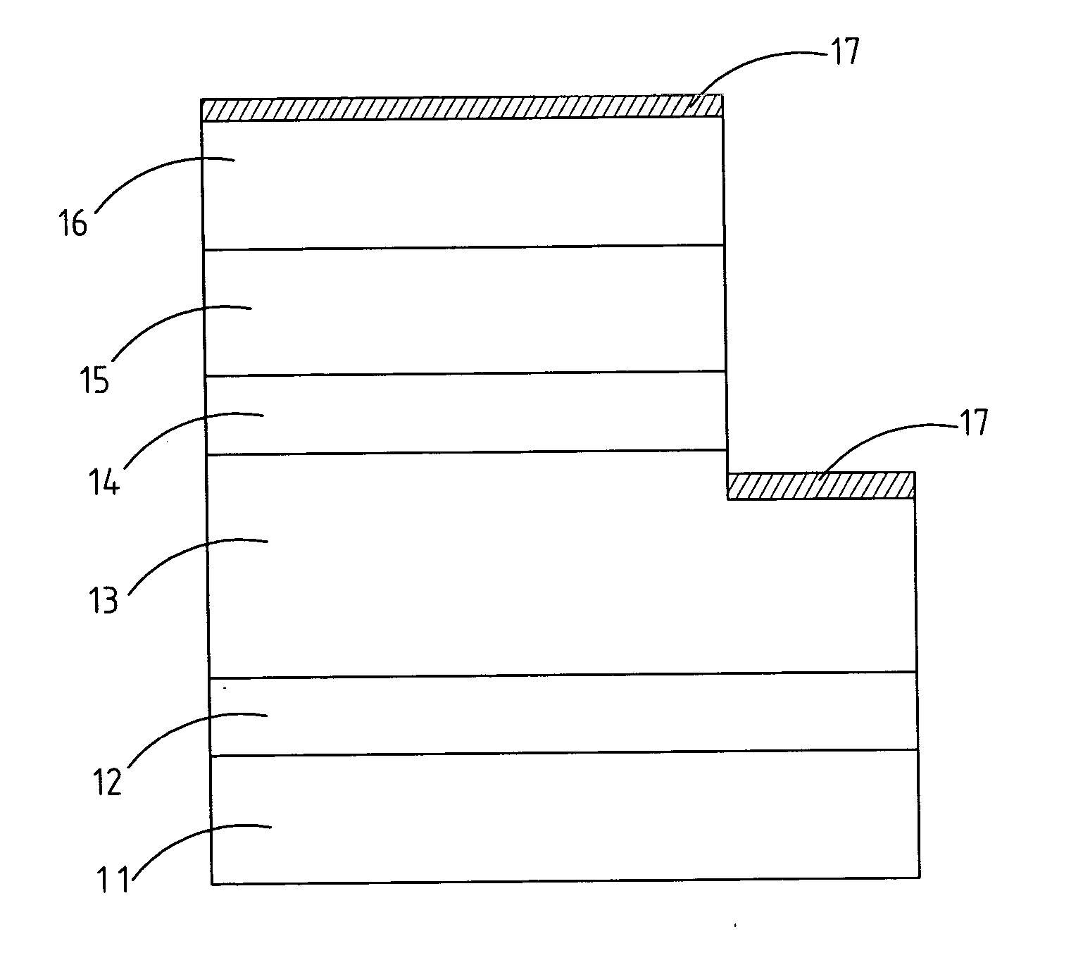
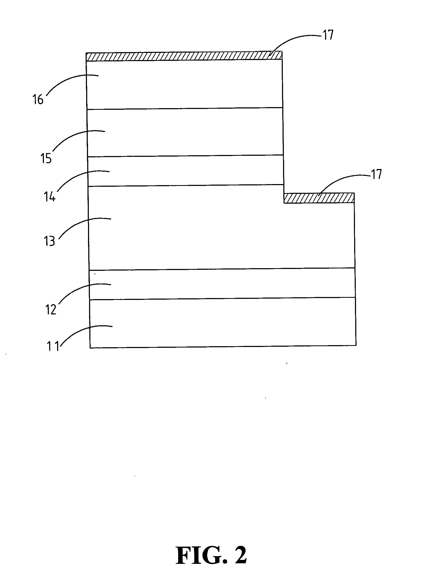
[0014]FIG. 2 is a schematic diagram showing the GaN-based LED structure according to the present invention.

[0015] As shown in FIG. 2, the GaN-based LED structure contains a substrate 11, a buffer layer 12, a n-type GaN contact layer 13, an active layer 14, a p-type cladding layer 15, and a p-type contact layer 16.

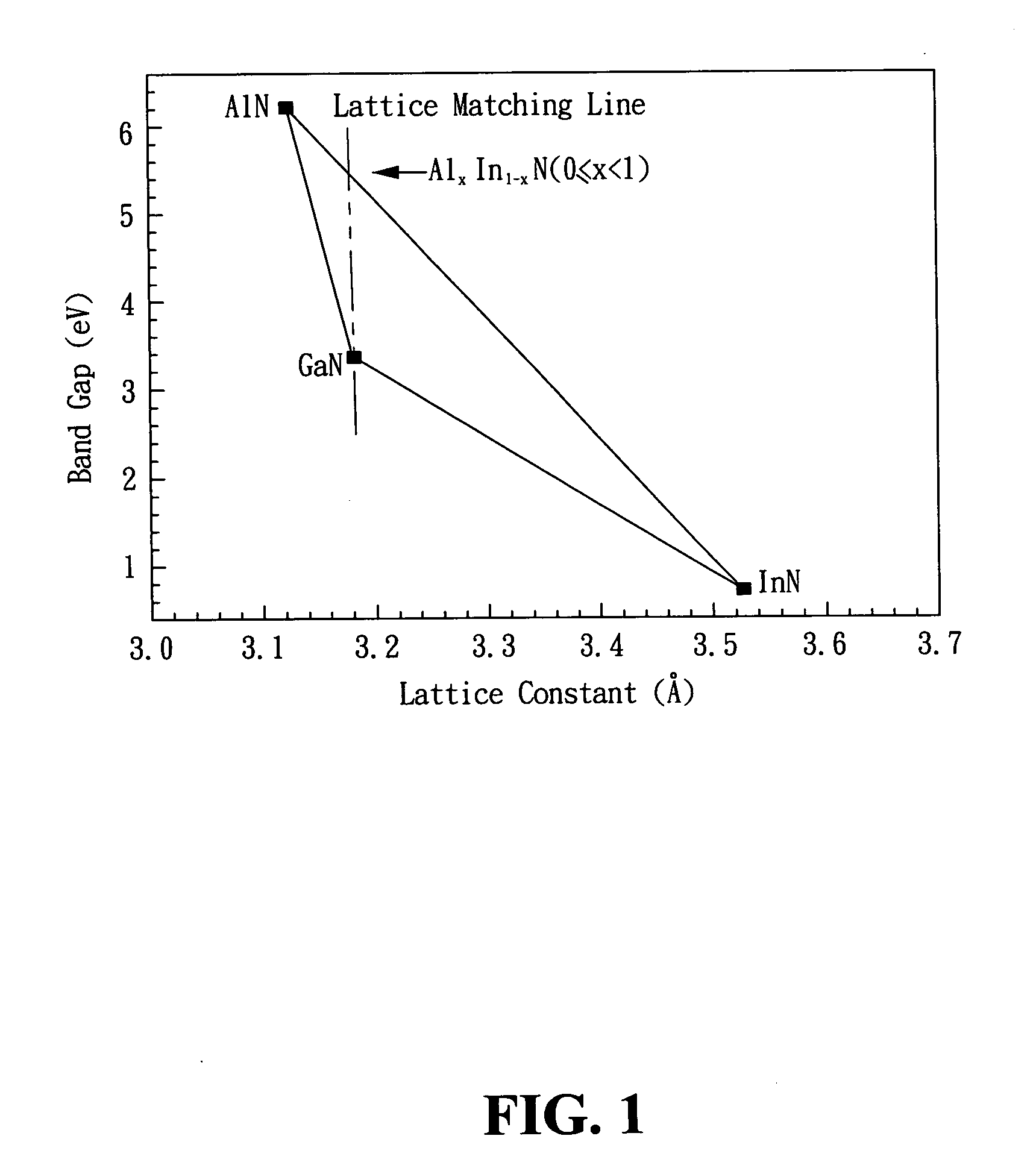
[0016] The substrate 11 is made of sapphire (aluminum-oxide monocrystalline). The buffer layer 12 is located upon the substrate 11 and is made of aluminum-gallium-indium-nitride (Al1-a-bGaaInbN, 0≦a, b13 is located upon the buffer layer 12. The active layer 14 is located upon the n-type GaN contact layer 13 and is made of InGaN. The p-type cladding layer 15 on top of the active layer 14 is made of magnesium (Mg)-doped Al1-cIncN (015 is grown under a temperature between 600° C. and 1200° C.

[0017] The p-type contact layer 16 on top of the p-type cladding layer 15 is made of Mg-doped GaN.

[0018] As shown in FIG. 2, the GaN-based LED structure according to the first embodimen...

second embodiment

[0019]FIG. 3 is a schematic diagram showing the GaN-based LED structure according to the present invention.

[0020] As shown in FIG. 3, the GaN-based LED structure contains a substrate 21, a buffer layer 22, a n-type GaN contact layer 23, an active layer 24, a p-type cladding layer 25, and a p-type contact layer 26.

[0021] The substrate 21 is made of sapphire (aluminum-oxide monocrystalline). The buffer layer 22 is located upon the substrate 21 and is made of Al1-d-eGadIneN (0≦d, e23 is located upon the buffer layer 22. The active layer 24 is located upon the n-type GaN contact layer 23 and is made of InGaN. The p-type cladding layer 25 on top of the active layer 24 is made of Al1-fInfN (025 is grown under a temperature between 600° C. and 1200° C.

[0022] The p-type contact layer 26 on top of the p-type cladding layer 25 is made of Mg-doped GaN.

[0023] As shown in FIG. 3, the GaN-based LED structure according to the second embodiment of the present invention can further contain an ele...

third embodiment

[0024]FIG. 4 is a schematic diagram showing the GaN-based LED structure according to the present invention.

[0025] As shown in FIG. 4, the GaN-based LED structure contains a substrate 31, a buffer layer 32, a n-type GaN contact layer 33, an active layer 34, a p-type double cladding layer 35, and a p-type contact layer 36.

[0026] The substrate 31 is made of sapphire (aluminum-oxide monocrystalline). The buffer layer 32 is located upon the substrate 31 and is made of Al1-g-hGagInhN (0≦g, h33 is located upon the buffer layer 32. The active layer 34 is located upon the n-type GaN contact layer 33 and is made of InGaN. The p-type double cladding layer 35 on top of the active layer 34 further contains a first cladding layer 351 and a second cladding layer 352. The first cladding layer 351 on top of the active layer 34 is made of Al1-iIniN (0351 is grown under a temperature between 600° C. and 1200° C. The second cladding layer 352 on top of the first cladding layer 351 is made of Mg-doped ...


PUM


Abstract

A gallium-nitride(GaN) based light emitting diode (LED) structure utilizing materials having compatible lattice constant is provided. When aluminum-indium-nitride (AlxIn1-xN, 0<x<1) is used to make the p-type cladding layer within the GaN-based LED structure, the cladding layer has a lattice constant compatible with that of GaN. The active layer's multi-quantum well (MQW) structure, therefore, would not be damaged from the excessive stress resulted from the incompatible lattice constant during the GaN-based LED's epitaxial growth. In addition, AlxIn1-xN (0<x<1) has a wider band gap than that of GaN, which can prevent electrons from overflowing from the MQW active layer. This, in turn, will increase the possibility of forming electron-hole pairs within the MQW active layer. Also due to its wider band gap, AlxIn1-xN (0<x<1) has an effective confinement effect on the photons, which again will increase the GaN-based LED's lighting efficiency. Besides, AlxIn1-xN (0<x<1) has a lower growing temperature so that the MQW active layer would remain intact during the low-temperature growth of the cladding layer, which, again, would increase the GaN-based LED's lighting efficiency.

Description

BACKGROUND OF THE INVENTION [0001] 1. Field of the Invention [0002] The present invention relates to the gallium-nitride (GaN) based light emitting diode (LED), and in particular to the epitaxy structure of the GaN-based LED. [0003] 2. The Prior Arts [0004] Conventionally, a GaN-based LED utilizing indium-gallium-nitride (InGaN) multi-quantum wells (MQWs) technology usually employs a structure whose InGaN MQW active layer is covered and protected by a p-type aluminum-gallium-nitride (AlGaN) cladding layer. Based on the observation from practical operations, however, such a structure has a number of disadvantages. The two severest ones are as follows. First, the lattice constant of the p-type AlGaN cladding layer is very much different from that of the InGaN MQW active layer. Such a significant difference in lattice constants, due to the piezoelectric field effect, would easily cause a stress so strong that the light emitting characteristics of the LED's epitaxy structure is affected...

Claims


Application Information

Patent Timeline
IPC IPC(8): H01L33/00H01L33/12H01L33/14H01L33/32
CPCH01L33/12H01L33/32H01L33/14
Inventor WU, LIANG-WENTU, RU-CHINYU, CHENG-TSANGWEN, TZU-CHICHIEN, FEN-REN
Owner FORMOSA EPITAXY INCORPORATION
Why Eureka
Try Eureka