Semiconductor device, semiconductor module, and manufacturing method of semiconductor device

Inactive Publication Date: 2006-03-02
SHARP KK
View PDF8 Cites 32 Cited by
  • Summary
  • Abstract
  • Description
  • Claims
  • Application Information

AI Technical Summary

Benefits of technology

[0008] The present invention has been made with the aim of solving the above problem, and it is an object of the present invention to provide a semiconductor device and a semiconductor module where a semiconductor substrate and a covering section for covering the semiconductor substrate are bonded to each other by an adhesive layer of which the water vapor permeability ranges from 10 g/(m2·2

Problems solved by technology

However, in the technology disclosed in Japanese Patent Application Laid Open No. 03-151666 (1991), there is a problem that the adhesive used for bonding the cap glass 102 to the chip 100 permits moisture to enter the inter

Method used


Image

  • Semiconductor device, semiconductor module, and manufacturing method of semiconductor device
  • Semiconductor device, semiconductor module, and manufacturing method of semiconductor device
  • Semiconductor device, semiconductor module, and manufacturing method of semiconductor device

Examples


Example

Embodiment 1

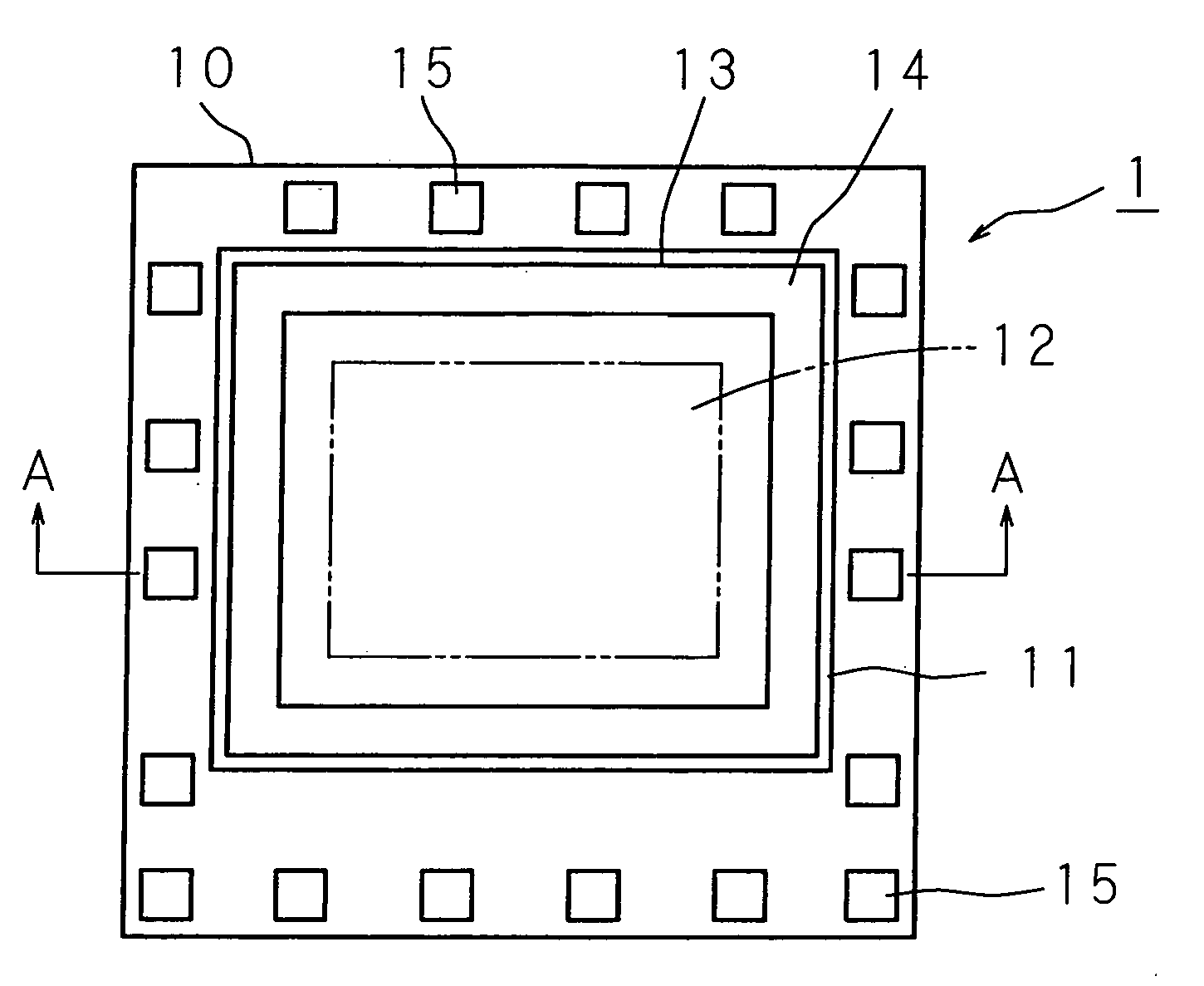
[0079]FIGS. 3A and 3B illustrate a schematic arrangement of the imaging device as a semiconductor device according to Embodiment 1 of the present invention. More specifically, FIG. 3A is a plan view (from above) of the imaging device and FIG. 3B is a structure cross sectional view taken along the line A-A of FIG. 3A.

[0080] The imaging device 1 as a semiconductor device according to Embodiment 1 of the present invention comprises a semiconductor substrate 10 on which an imaging element 11 is disposed of a rectangular shape when shown from above, a lid section 13 provided opposite to a light receiving section 12 at one surface of the imaging element 11, and an adhesive layer 14 provided on the one surface, except the light receiving section 12, of the imaging device 11 for bonding between the semiconductor substrate 10 (the imaging element 11) and the lid section 13.

[0081] The imaging device 1 is designed for taking in the incident light passed through the lid section 1...

Example

Embodiment 2

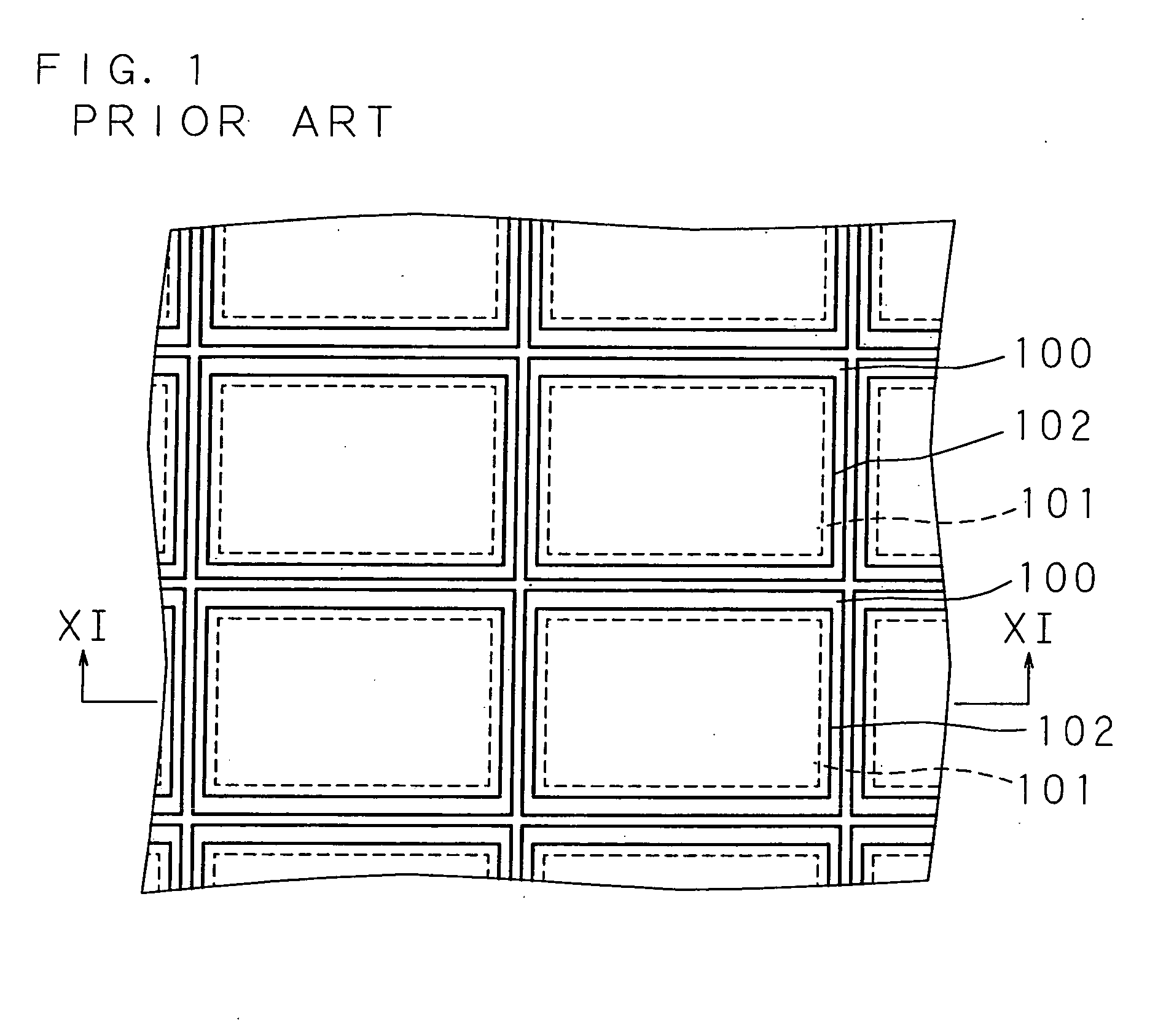
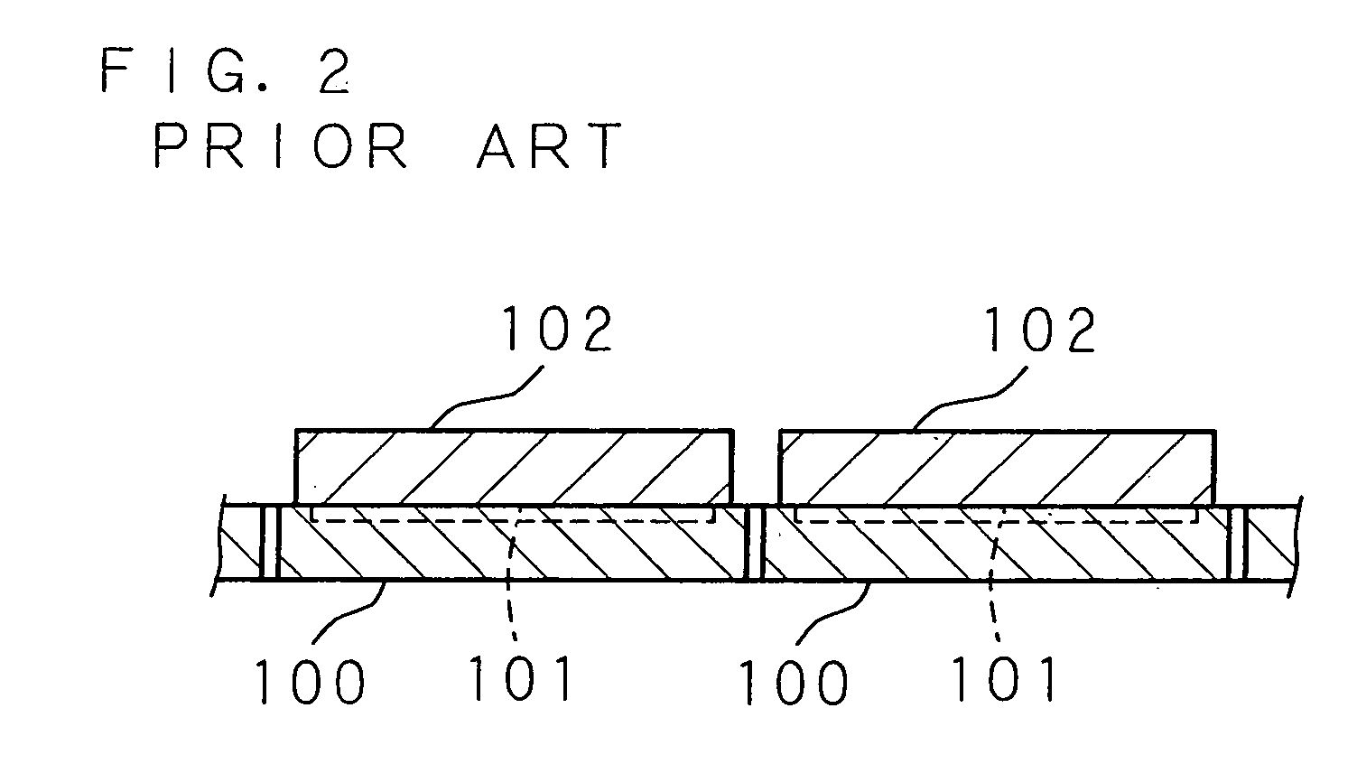
[0120]FIGS. 9A, 9B, 10A, 10B, and 10C illustrate a manufacturing method of the imaging device as a semiconductor device according to Embodiment 2 of the present invention. More particularly, FIGS. 9A and 9B are explanatory views showing the adhesive layer provided on one surface (including the light receiving section) of each of imaging elements on the semiconductor wafer. FIGS. 10A to 10C are explanatory views showing steps of bonding a light-transmitting plate material on the semiconductor wafer shown in FIGS. 9A and 9B and separating the light-transmitting plate material to develop the lid sections of the imaging devices.

[0121]FIG. 9A illustrates the adhesive layer 14 patterned, in a peripheral area except the light receiving section 12, on the surface (including the light receiving sections 12) of each of the imaging elements 11 on the semiconductor wafer 30. FIG. 9B is a structure cross sectional view taken along the line A-A of FIG. 9A. The illustrations are iden...

Example

Embodiment 3

[0127]FIG. 11 is a structure cross sectional view of a schematic arrangement of a semiconductor module according to Embodiment 3 of the present invention. The semiconductor module 2 may be a camera module where a lens 41 for focusing the incident light and a lend holder 42 for holding the lens 41 are mounted on a wiring substrate 40 such as a printed circuit board or a ceramic board. Also, a digital signal processor 43 (referred to as a DSP hereinafter) is provided on the wiring substrate 40. The DSP 43 functions as a controller (image processing apparatus) for controlling the action of the imaging device 1 (imaging element 11) and converting output signals of the imaging device 1 (imaging element 11) into relevant signals which can commonly be used in an optical apparatus. The DSP 43 is electrically connected at its connecting terminals by bonding wires 43w to corresponding a wiring (not shown) on the wiring substrate 40.

[0128] The imaging device 1 acting as the semic...


PUM


Abstract

An imaging device as a semiconductor device includes a semiconductor substrate on which an imaging element is mounted, a light-transmitting lid section (covering section) arranged to face a light receiving section provided on one surface of the imaging element, and an adhesive layer arranged in an area excluding the light receiving section on the one surface of the imaging element for bonding between the semiconductor substrate and the lid section. The adhesive layer ranges from 10 g/(m2·24 h) to 200 g/(m2·24 h) in the water vapor permeability.

Description

CROSS-REFERENCE TO RELATED APPLICATIONS [0001] This nonprovisional application claims priority under 35 U.S.C. §119(a) on Patent Application No. 2004-251235 filed in Japan on Aug. 31, 2004, the entire contents of which are hereby incorporated by reference. BACKGROUND OF THE INVENTION [0002] 1. Field of the Invention [0003] The present invention relates to a semiconductor device having a semiconductor substrate provided with a covering section, a semiconductor module employing the semiconductor device, and a manufacturing method of the semiconductor device. More particularly, the present invention relates to a semiconductor device in which a space provided between its semiconductor substrate and covering section is protected at the interior from condensation, a semiconductor module, and a manufacturing method of the semiconductor device. [0004] 2. Description of Related Art [0005] Imaging devices such as an area sensor or a linear sensor including an imaging element such as a CCD or ...

Claims


Application Information

Patent Timeline
IPC IPC(8): H01L23/495H01L23/02H01L23/10H01L23/28H01L27/14H04N5/335H04N5/369
CPCH01L27/14618H01L27/1462H01L27/14625H01L27/14685H01L31/0203H01L2224/73265H01L2224/48091H01L2924/00014H01L27/146
Inventor TSUKAMOTO, HIROAKIFUJITA, KAZUYAYASUDOME, TAKASHI
Owner SHARP KK
Why Eureka
Try Eureka