

Positive resist composition and pattern forming method utilizing the same
a composition and resist technology, applied in the direction of auxillary/base layers of photosensitive materials, instruments, photosensitive materials, etc., can solve the problem of not finding a resist composition capable of meeting the aforementioned requirements, and achieve excellent in-plane uniform line width and excellent lwr property
- Summary
- Abstract
- Description
- Claims
- Application Information
AI Technical Summary
Benefits of technology
Problems solved by technology
Method used
Image

Examples
synthesis example 1
Synthesis of Resin (1))
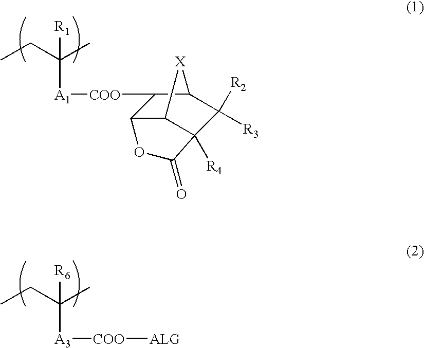
[0319] 9-methacryloyloxy-5-methyl-2-oxatricyclo[4.2.1.04.8]nonan-3-one, 2-methyl-2-adamantyl methacrylate, and methacrylic acid were charged in a proportion of 44 / 50 / 6 (molar ratio), dissolved in propylene glycol monomethyl ether acetate (PGMEA) / propylene glycol monomethyl ether (PGME)=60 / 40 (weight ratio), to obtain 450 g of a solution of a solid concentration of 22 weight %. The solution was added with a polymerization initiator V-601 (dimethyl-2,2′-azobis(2-methylpropionate)), manufactured by Wako Pure Chemicals Industries Inc., by 8 mol and was dropwise added, over 6 hours and in a nitrogen atmosphere, to 50 g of a mixed solution of PGMEA / PGME=60 / 40 (weight ratio), heated to 80° C. After the addition, the reaction liquid was agitated for 2 hours. After the reaction, the reaction liquid was cooled to the room temperature and poured into 5 L of a mixed solvent of hexane / ethyl acetate=9 / 1 (weight ratio), and precipitated white powder was separated by filteri...
PUM
| Property | Measurement | Unit |
|---|---|---|
| temperature | aaaaa | aaaaa |
| temperature | aaaaa | aaaaa |
| temperature | aaaaa | aaaaa |
Abstract
Description
Claims
Application Information