Semiconductor integrated device

a technology of integrated devices and semiconductors, applied in the direction of semiconductor devices, basic electric elements, electrical equipment, etc., can solve the problems of low potential holes in the body, difficult fabrication of semiconductor devices, and inability to secure the stabilizing capacitor formed between the body and the supporting substra

Inactive Publication Date: 2006-03-02
KK TOSHIBA
View PDF7 Cites 58 Cited by
  • Summary
  • Abstract
  • Description
  • Claims
  • Application Information

AI Technical Summary

Benefits of technology

[0022] wherein the first and second well diffusion regions are set to prescribed potentials, respectively, in order to avoid inversion of conduction type at a side near to the embedded insulation film in a region sandwiched by a channel region of the NMOSFET, a channel region of the PMOSFET and the embedded insulation film.

Problems solved by technology

As for the conventional DRAM cell consisted of one transistor and one capacitor including a trench capacitor or a stacked capacitor, there is a concern that its fabrication may become difficult as it becomes finer.
However, holes are stored in the body having a low potential.
If the film thickness of a buried oxide film is thick, however, it becomes impossible to secure a stabilizing capacitor formed between a body and a support substrate.
This results in a problem that the signal quantity of the memory cells cannot be made large.
In forming such a bipolar transistor on a support substrate under the buried oxide film of SOI, however, it becomes difficult to form contacts if the buried oxide film is thick.

Method used


Image

  • Semiconductor integrated device
  • Semiconductor integrated device
  • Semiconductor integrated device

Examples


first embodiment

(First Embodiment)

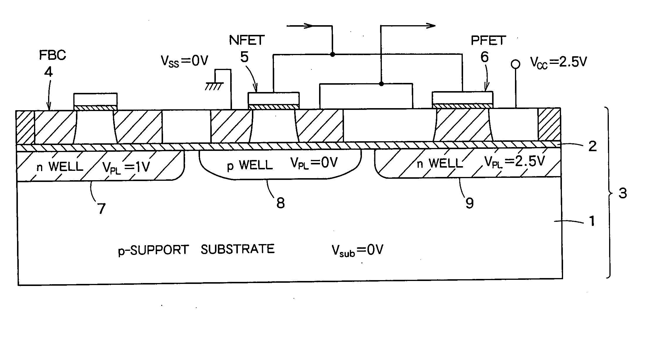
[0061]FIG. 1 is a sectional view of a semiconductor integrated device according to a first embodiment of the present invention. In the semiconductor integrated device in FIG. 1, a sectional structure of a peripheral circuit of a semiconductor storage device using FBCs as memory cells is shown.

[0062] In the present embodiment, a SOI substrate 3 including a p-support substrate 1 and a buried oxide film 2 formed as a thin film are used. By forming the buried oxide film 2 as a thin film, the signal quantity of the FBCs can be sufficiently ensured and the data retention time can be prolonged.

[0063] In FIG. 1, an FBC 4, an NFET 5 and a PFET 6 are formed on a top surface of the buried oxide film 2 in the SOI substrate 3 so as to be separated from each other. An n-well diffused region 7 is formed in contact with the buried oxide film 2, in the p-support substrate 1 located under the FBC 4. A p-well diffused region 8 is formed in the p-support substrate 1 located under th...

second embodiment

(Second Embodiment)

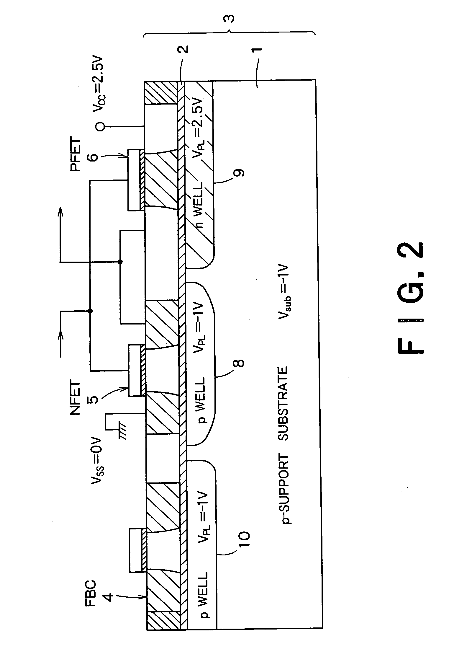
[0071] In a second embodiment, a back channel is prevented from being formed when a voltage lower than 0 V is applied to the p-support substrate 1 in the SOI substrate 3.

[0072]FIG. 3 is a sectional view of a semiconductor integrated device according to a second embodiment of the present invention. In the same way as FIG. 1, the semiconductor integrated device shown in FIG. 3 includes an FBC 4, an NFET 5 and a PFET 6 formed on a SOI substrate 3 including a p-support substrate 1 and a buried oxide film 2 formed as a thin film, so as to be separated from each other.

[0073] In the same way as FIG. 1, an n-well diffused region 7 is formed in the p-support substrate 1 located under the FBC 4. A p-well diffused region 8 is formed in the p-support substrate 1 located under the NFET 5. Furthermore, an n-well diffused region 11 is formed so as to be adjacent to the p-well diffused region 8. An n-well diffused region 12 is formed beneath bottom surfaces of the n-well diffus...

third embodiment

(Third Embodiment)

[0078] In the first and second embodiments, the SOI substrate 3 including the p-support substrate 1 is used. However, a SOI substrate 3 including an n-support substrate may be used.

[0079] In this case, a structure corresponding to FIG. 1 becomes as shown in FIG. 5. A semiconductor integrated device shown in FIG. 5 includes an n-well diffused region formed under an FBC 4, a p-well diffused region 8 formed under an NFET 5, an n-well diffused region 9 formed under a PFET 6, and a p-well diffused region 13 formed on a bottom surface side of the p-well diffused region 8 and the n-well diffused region 9.

[0080] An n-support substrate 20 is set to a voltage Vsub=0 V. A voltage VPL=0 V is applied to the n-well diffused region 7. The p-well diffused region 8 is set to a voltage VPL=0 V. A voltage VPL=2.5 V is applied to the n-well diffused region 9. The p-well diffused region 13 is provided to prevent a short-circuit between the n-well diffused region 9 and the n-support s...


PUM


Abstract

A semiconductor integrated apparatus, comprising: an SOI (Silicon On Insulator) substrate which has a support substrate and an embedded insulation film; an NMOSFET, a PMOSFET and an FBC (Floating Body Cell) formed on the SOI substrate separately from each other; a p type of first well diffusion region formed along the embedded insulation film in the support substrate below the NMOSFET; an n type of second well diffusion region formed along the embedded insulation film in the support substrate below the PMOSFET; and a conduction type of third well diffusion region formed along the embedded insulation film in the support substrate below the FBC.

Description

CROSS REFERENCE TO RELATED APPLICATIONS [0001] This application is based upon and claims the benefit of priority from the prior Japanese Patent Application No. 2004-252757, filed on Aug. 31, 2004, the entire contents of which are incorporated herein by reference. BACKGROUND OF THE INVENTION [0002] 1. Field of the Invention [0003] The present invention relates to a semiconductor integrated device including well diffused regions formed in a SOI (Silicon on Insulator) substrate. [0004] 2. Related Art [0005] As for the conventional DRAM cell consisted of one transistor and one capacitor including a trench capacitor or a stacked capacitor, there is a concern that its fabrication may become difficult as it becomes finer. As a candidate for a future DRAM cell, a new memory cell FBC (Floating Body Cell) is proposed (see Japanese Patent Application Laid-Open Nos. 2003-68877 and 2002-246571). In the FBC, majority carriers are stored in a floating body of an FET (Field Effect Transistor) forme...

Claims


Application Information

Patent Timeline
Patent Type & Authority Applications(United States)
IPC IPC(8): H01L21/331
CPCH01L27/1203H01L29/8611H01L29/735H01L29/7322
Inventor OHSAWA, TAKASHI
Owner KK TOSHIBA
Why Eureka
Try Eureka