Sealing of electronic device using absorbing layer for glue line

a technology of electronic devices and glue lines, applied in the direction of thermoelectric devices, solid-state devices, basic electric elements, etc., can solve the problems of components warping, damage to absorb ir radiation supplied,

Active Publication Date: 2006-03-09
DOLYA HOLDCO 5 LTD
View PDF2 Cites 63 Cited by
  • Summary
  • Abstract
  • Description
  • Claims
  • Application Information

AI Technical Summary

Benefits of technology

[0004] An embodiment of an encapsulated organic electronic device is described that includes: a substrate, an organic electronic device on the substrate, and a heat-activated adhesive that is on the substrate and surrounds a perimeter of the organic electronic device. The electronic device also includes an encapsulation cover that is on the heat-activated adhesive. A first absorbing layer is between the substrate and the heat-activated adhesive and is in proximity to the adhesive. In addition or alternatively, a second absorbing layer is between the encapsulation cover and the adhesiv...

Problems solved by technology

The absorption of the supplied IR radiation can damage, for example, the organic active layers of the electronic device, the substrate, and/or the enca...

Method used


Image

  • Sealing of electronic device using absorbing layer for glue line
  • Sealing of electronic device using absorbing layer for glue line
  • Sealing of electronic device using absorbing layer for glue line

Examples


Embodiment Construction

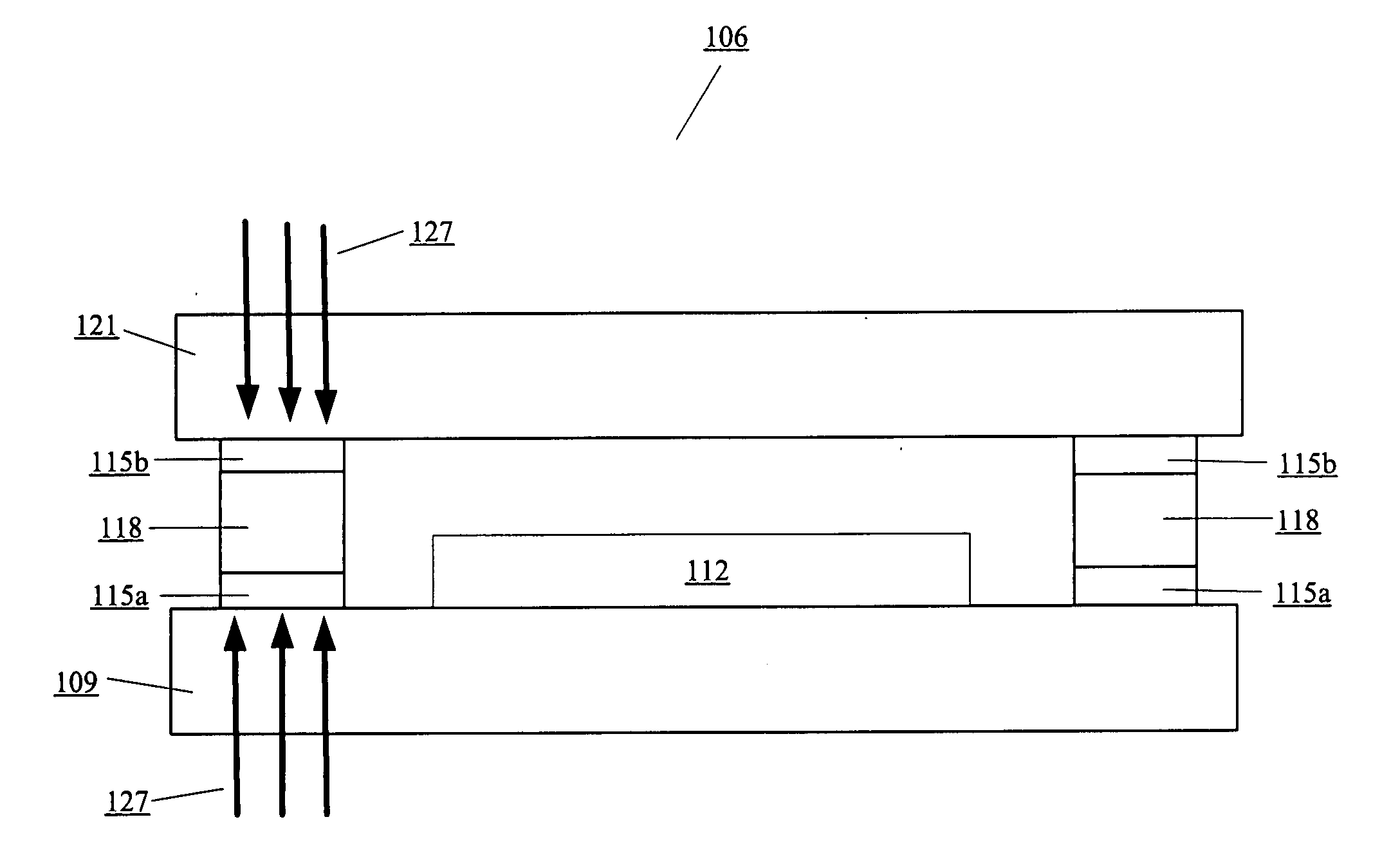
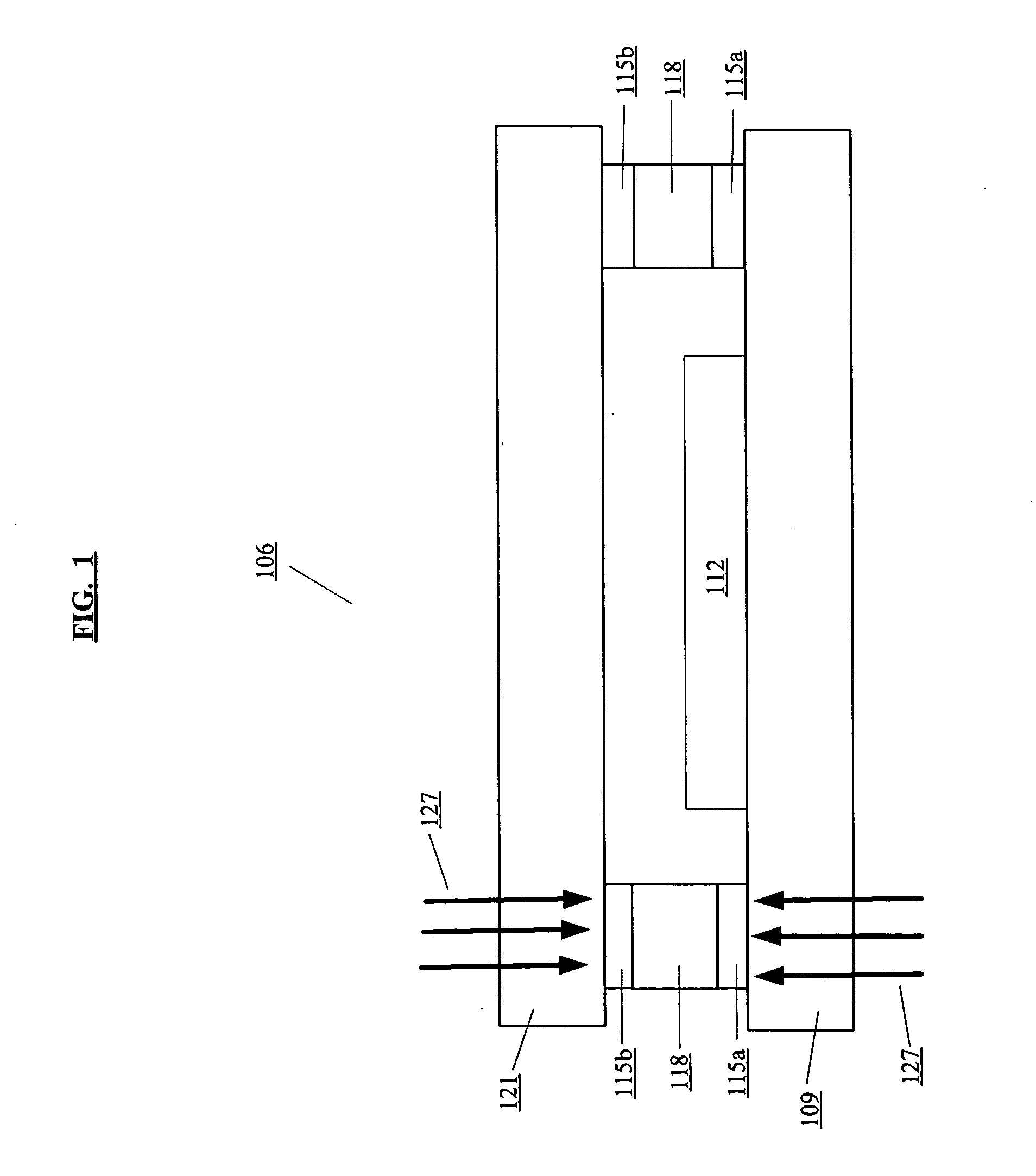
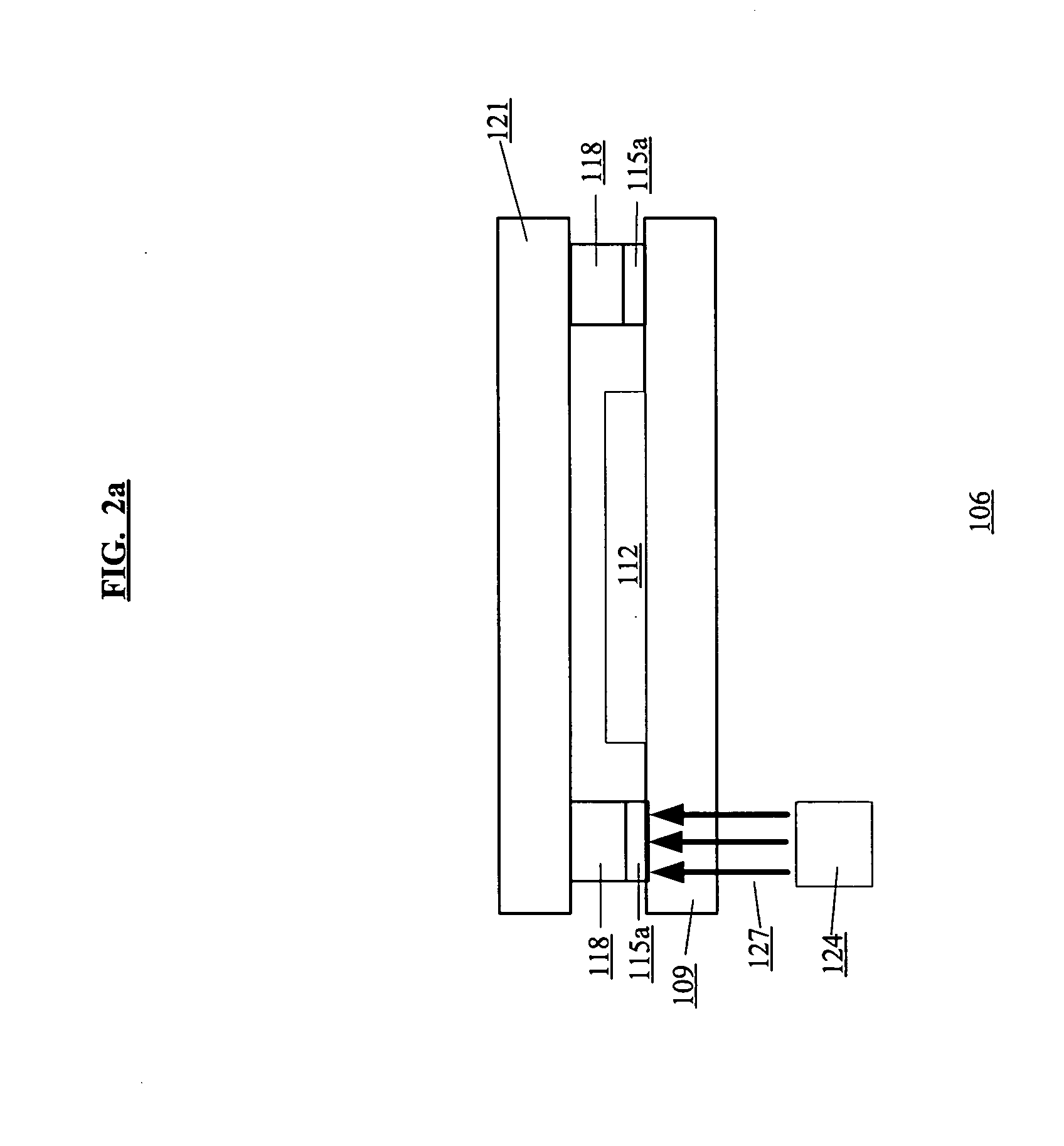
[0017] In an embodiment of this invention, a first absorbing layer is on a substrate and / or a second absorbing layer is on a heat-activated adhesive. If the IR source that supplies IR radiation is present on a substrate-side, then an absorption percentage of the substrate is less than an absorption percentage of the first absorbing layer if present and less than an absorption percentage of the second absorbing layer if present. If the IR source that supplies IR radiation is present on an “encapsulation cover”-side, then an absorption percentage of the encapsulation cover is less than an absorption percentage of the first absorbing layer if present and less than an absorption percentage of the second absorbing layer if present. The substrate and the encapsulation cover have a low thermal conductivity. When the substrate and the encapsulation cover are brought together so as to seal the organic electronic device, the first absorbing layer if present is in proximity to the heat-activat...


PUM


Abstract

In one embodiment of the invention, a first absorbing layer is on a substrate and/or a second absorbing layer is on a heat-activated adhesive. If the IR source that supplies IR radiation is present on the substrate-side, then the absorption percentage of the substrate is less than the absorption percentage of the first absorbing layer if present and less than the absorption percentage of the second absorbing layer if present. If the IR source that supplies IR radiation is present on the “encapsulation cover”-side, then the absorption percentage of the encapsulation cover is less than the absorption percentage of the first absorbing layer if present and less than an absorption percentage of the second absorbing layer if present. The substrate and the encapsulation cover have a low thermal conductivity.

Description

BACKGROUND OF THE INVENTION [0001] An organic electronic device such as, for example, an organic light emitting diode (“OLED”) display, an OLED light source for area illumination, an organic light sensor array, an organic transistor array, or an organic solar cell array require protection from oxygen and moisture in the atmosphere, and therefore employ some form of encapsulation. One common procedure to encapsulate the organic electronic device is to sandwich it between a substrate and an encapsulation cover, and an adhesive around the perimeter of the device holds together the substrate and the encapsulation cover such that there is a continuous perimeter seal around the device. [0002] Typically, the substrate and the encapsulation cover are sealed together using UV-curable adhesive or thermal-cure adhesive. In many cases, use of the thermal-cure adhesive would be advantageous. Thermal-cure adhesive provides many advantages such as good performance and predictable results due to th...

Claims


Application Information

Patent Timeline
IPC IPC(8): H01L29/08
CPCH01L21/50H01L23/10H01L51/448H01L51/5237H01L2924/0002Y02E10/549H01L2924/00H10K30/88H10K50/8426H10K50/844
Inventor PICHLER, KARLFRISCHKNECHT, KYLE D.
Owner DOLYA HOLDCO 5 LTD
Why Eureka
Try Eureka