Decoder of semiconductor memory device

Inactive Publication Date: 2006-03-09
LAPIS SEMICON CO LTD
View PDF5 Cites 0 Cited by
  • Summary
  • Abstract
  • Description
  • Claims
  • Application Information

AI Technical Summary

Benefits of technology

[0027] According to the decoder of the semiconductor memory device of the invention, at the time of a defect test of a normal (ordinary) memory cell, the redundant memory cells can be continuously accessed after the access to the normal memory cell. Since there is, consequently, no need to separately execute the redundant cell test and to access the unnecessary memory cells, the testing time can be shortened.
[0028] According to the decoder of another semiconductor memory device of the invention, only the redundant memory cells can be sequentially accessed irrespective of the status of the column address. Since there is, consequently, no need to access the unnecessary memory cells at the time of the redundant cell test, the testing time can be shortened.

Problems solved by technology

In the semiconductor memory device as shown in FIG. 1 such as conventional FIFO memory or serial register in which the address setting cannot be performed and only the serial access can be executed, however, although the writing / reading operation can be serially executed from the head address in a memory space by a reset input in terms of a circuit construction, such an operation that the writing / reading is executed from an arbitrary address like a general DRAM (Dynamic Random Access Memory) or the like cannot be executed.
Since the whole memory space is, thus, accessed only for discrimination about the defect of the redundant memory cell 2s, there is a problem of an increase in testing time.

Method used


Image

  • Decoder of semiconductor memory device
  • Decoder of semiconductor memory device
  • Decoder of semiconductor memory device

Examples


embodiment 1

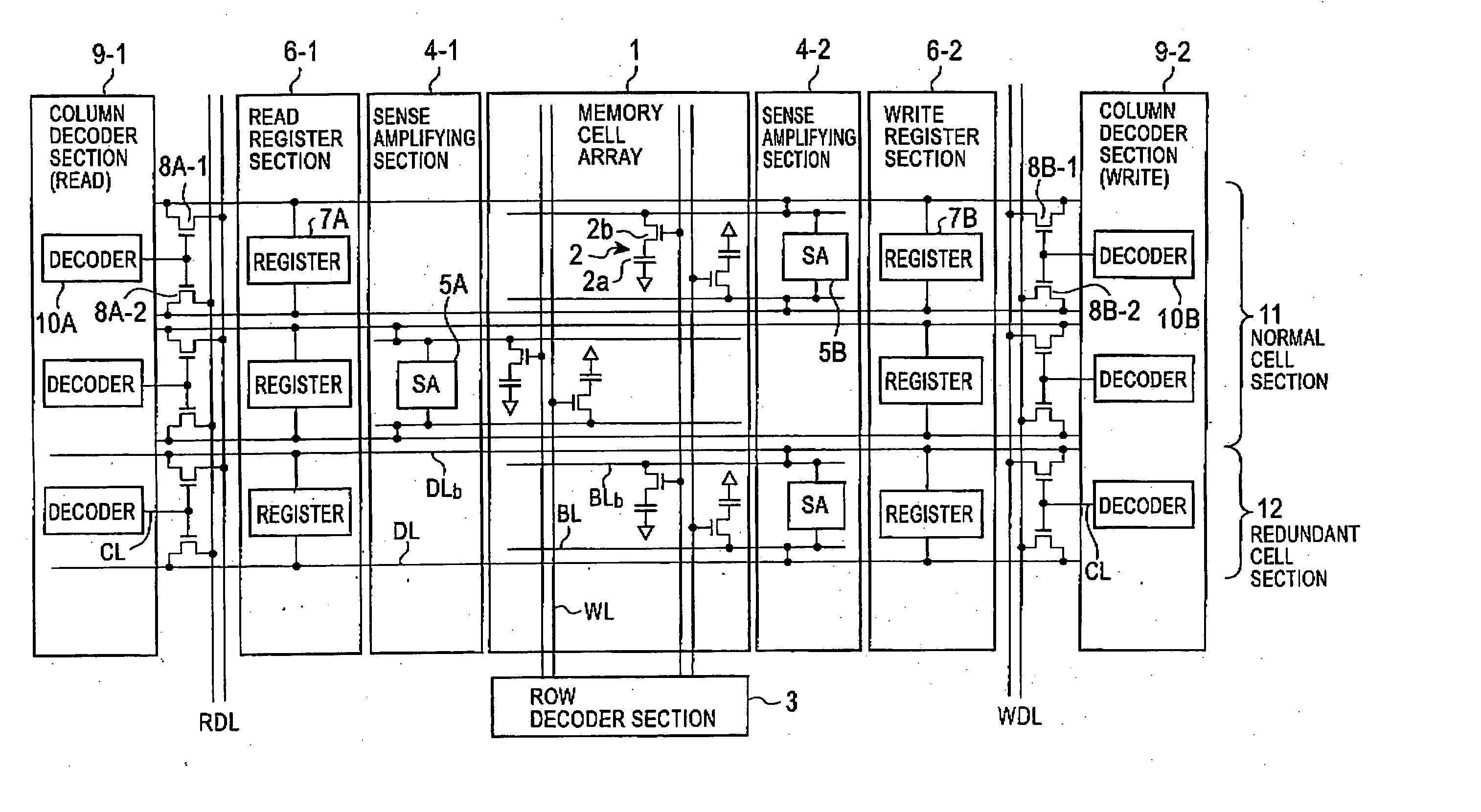
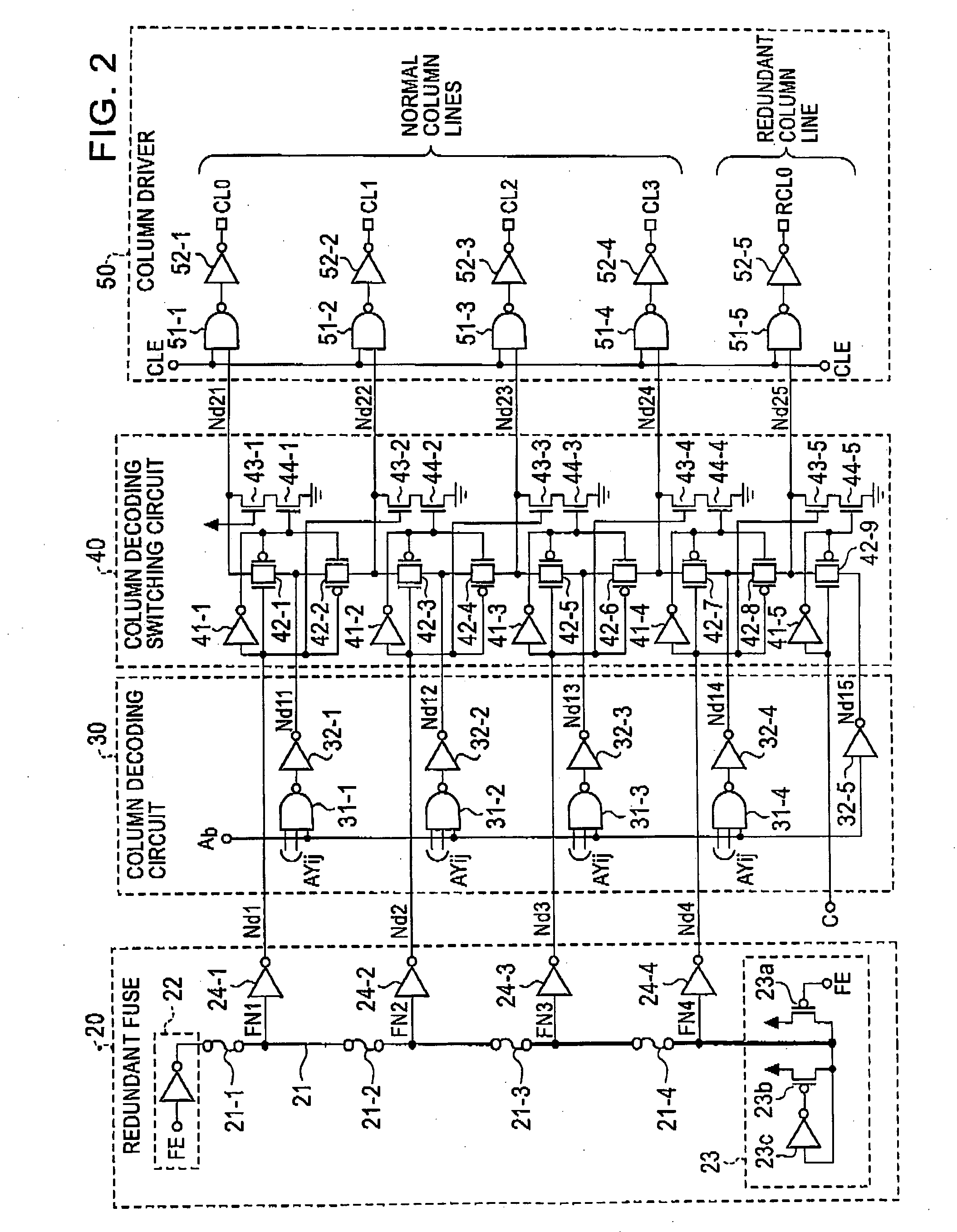
[0039]FIG. 2 is a schematic circuit diagram of a decoder in a column decoder in a semiconductor memory device of FIG. 1 showing the invention.

[0040] The decoder in FIG. 2 is a circuit corresponding to each of the decoders 10A and 10B constructing the column decoder sections 9-1 and 9-2 in FIG. 1. In FIG. 2, for simplicity of drawings, a constructional example having four normal column lines CL0 to CL3 and one redundant column line RCL0 is shown.

[0041] The decoder in FIG. 2 is mainly constructed by: a redundant fuse 20 for generating a redundant fuse signal; a column decoding circuit 30 for decoding a column address AYij; a column decoding switching circuit 40 for switching an output destination of a decoding result of the column decoding circuit 30 by the redundant fuse signal; and a column driver 50 for driving an output signal of the column decoding switching circuit 40 and supplying the driven output signal to the normal column lines CL0 to CL3 and the redundant column line RCL0...

embodiment 2

[0068]FIG. 6 is a schematic circuit diagram of a decoder in a column decoder in a semiconductor memory device showing the invention. FIG. 7 is a constructional diagram showing the whole circuit of FIG. 6.

[0069] In the decoder in FIG. 6, a column decoding circuit 30A having a construction different from that of the circuit 30 is provided in place of the column decoding circuit 30 in FIG. 2. In the column decoding circuit 30A, an inversion redundant cell test signal Cb is used in place of the redundant address signal Ab in FIG. 2, the redundant cell test signal C, the inverters 32-5 and 41-5, and the transfer gate 42-9 in FIG. 2 are omitted, and a second decoding portion (for example, 2-input NANDs 31-4A and 32-4A) is provided in place of the 3-input NANDs 31-4 and 32-4. The 2-input NAND 31-4A uses column address AYij as an input. Its output signal and the inversion redundant cell test signal Cb are supplied to the 2-input NAND 32-4A and an output side of the NAND 32-4A corresponds to...

embodiment 3

[0074] The invention is not limited to the foregoing embodiments 1 and 2 but various modifications are possible. For example, the following (a) and (b) can be given as an embodiment 3 as a modification. [0075] (a) The redundant fuse 20, the column decoding circuit 30 and 30A, the column decoding switching circuit 40, and the column driver 50 can be also constructed by circuit elements other than those shown in the diagram. [0076] (b) The decoder of the embodiment can be applied to a semiconductor memory device which has a construction other than that in FIG. 1 and in which the serial access can be performed.


PUM


Abstract

A column decoder in a semiconductor memory device in which address setting cannot be performed but only a serial access can be performed. The column decoder is constructed by: a redundant fuse for generating a redundant fuse signal; a column decoding circuit for decoding a column address; a column decoding switching circuit for switching an output destination of a decoding result of the column decoding circuit by the redundant fuse signal; and a column driver for driving an output signal of the column decoding switching circuit and generating it to normal column lines and a redundant column line. The column decoding circuit continuously makes the redundant column line operative after the operation of the normal column lines.

Description

BACKGROUND OF THE INVENTION [0001] 1. Field of the Invention [0002] The invention relates to a decoder in a semiconductor memory device such as FIFO (First-In First-Out) memory or serial register in which addresses cannot be accessed at random and only a serial access can be executed and memory cells of a dynamic type are used and, more particularly, to a testing circuit of redundant memory cells. [0003] 2. Description of Related Art [0004] Hitherto, as a redundancy circuit to rescue a defective memory cell in a semiconductor memory device, for example, a redundancy circuit is disclosed in Japanese Patent Kokai No. 6-203590 (patent document 1). [0005] In the patent document 1, in a nonvolatile semiconductor memory device of an electrically batch erasing type such as random access flash memory (for example, EPROM which can be erased by ultraviolet rays and is electrically writable), a technique regarding a word line redundancy circuit on the row side has been disclosed. [0006] In a s...

Claims


Application Information

Patent Timeline
IPC IPC(8): G11C7/00
CPCG11C8/10G11C29/848G11C11/4087G11C11/401
Inventor KUROKI, OSAMU
Owner LAPIS SEMICON CO LTD
Why Eureka
Try Eureka