Method for deposition onto a substrate and method for producing photo conductor

Inactive Publication Date: 2006-03-09
PANASONIC CORP
View PDF3 Cites 0 Cited by
  • Summary
  • Abstract
  • Description
  • Claims
  • Application Information

AI Technical Summary

Benefits of technology

[0011] The present invention takes these problems into consideration and has an objective of providing a method for deposition onto a substrate and a manufacturing method of a photo conductor that uses this method for deposition that can reduce uneven deposition onto individual substrates when depositing coatings onto a plurality of substrates and can also reduce unevenness in the coating thickness of the protective surface layer of each photo conductor when forming protective surface layers on a plurality of photo conductors.

Problems solved by technology

When depositing a coating onto a plurality of substrates using a plasma CVD method with conventional technology, a problem of uneven deposition onto the substrates occurs within the substrates or between the substrates due to a circulating condition of the raw gas used for the deposition or the positional relationship between the vacuum containers that hold the substrates.
The occurrence of this type of uneven deposition is the cause of further problems in substrates used for the photo conductor.
Namely, uneven deposition causes both unevenness in the coating thickness of the protective surface layer as well as unevenness in the sensitivity and residual potential of the photo conductor.
When this type of unevenness in the coating thickness of the protective surface layer occurs, problems such as uneven density and fogging in images formed on this photo conductor will occur.

Method used


Image

  • Method for deposition onto a substrate and method for producing photo conductor
  • Method for deposition onto a substrate and method for producing photo conductor
  • Method for deposition onto a substrate and method for producing photo conductor

Examples


first embodiment

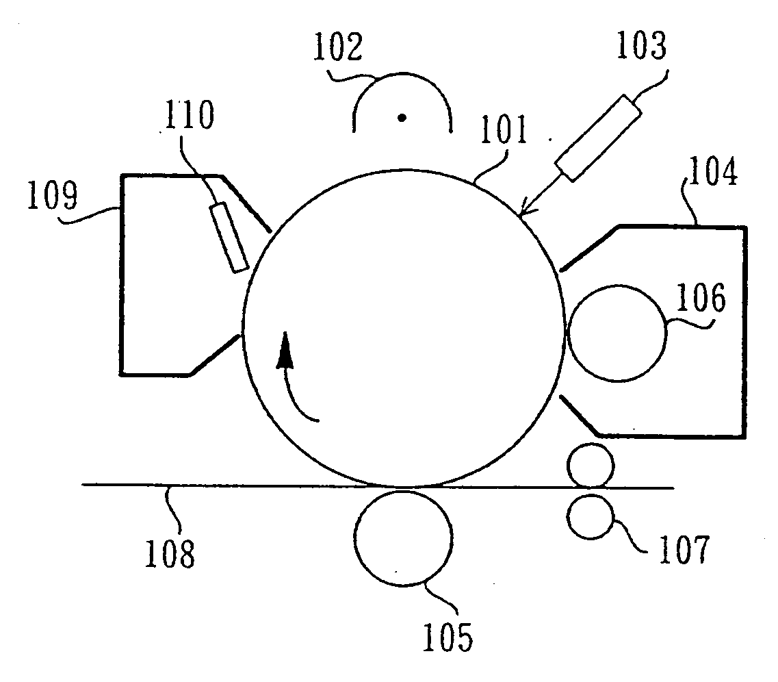
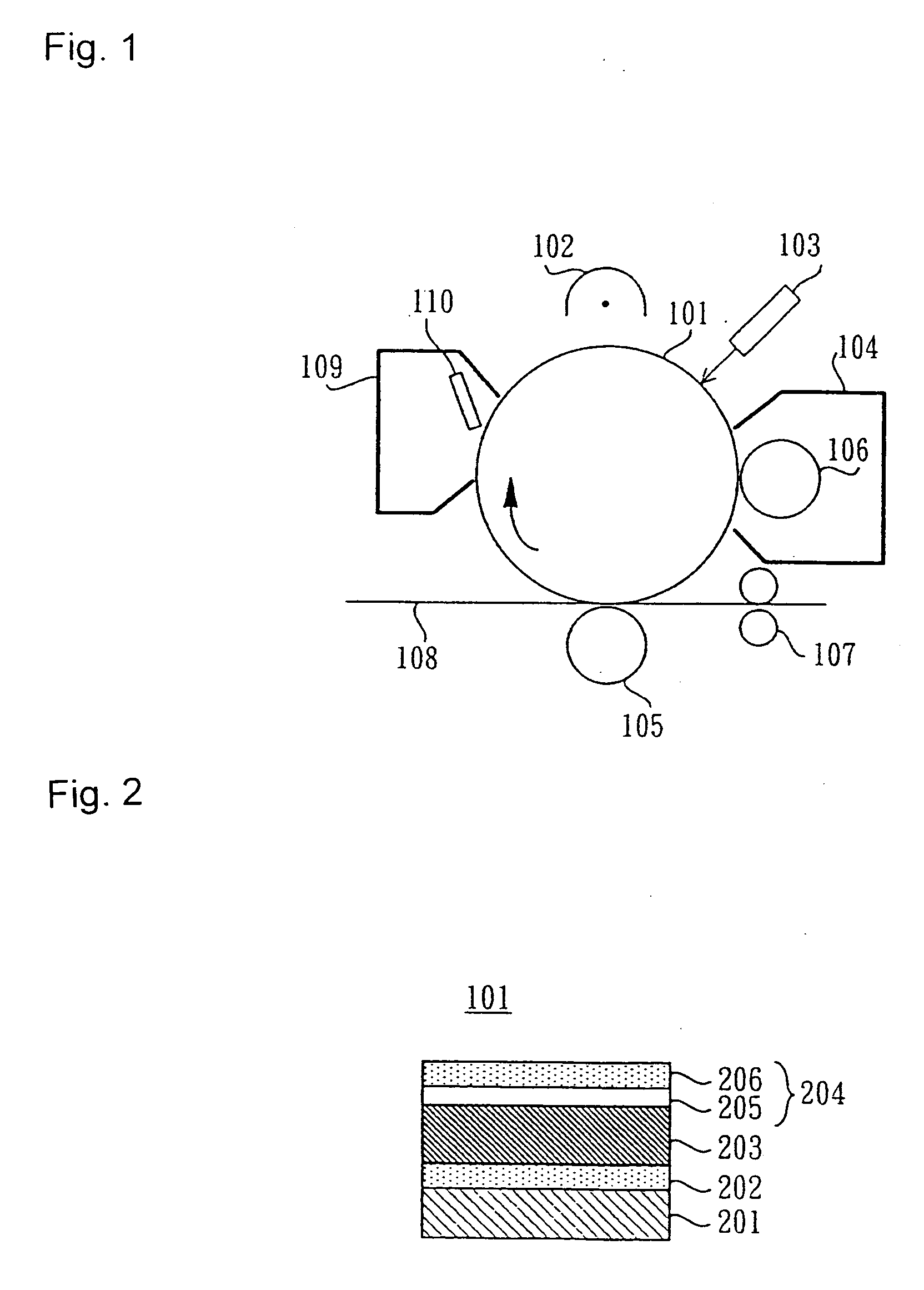
[0033]FIG. 1 shows the composition of the periphery of the image forming unit in an image forming apparatus wherein a photo conductor (hereinafter referred to as photosensitive material) is applied that utilizes a substrate deposited onto a substrate by the method for deposition related to the first embodiment of the present invention. Furthermore, in the following the member whereon a carrier generation layer and a carrier transport layer are deposited onto a conductive base material is referred to as a “substrate” in this specification.

[0034] As shown in this figure, an electric charging device 102 close to the photosensitive material 101, an exposure apparatus 103, a developing apparatus 104, and a transfer apparatus 105 are arranged in the related image forming apparatus. The photosensitive material 101 has a protective surface layer. The composition of the related protective surface layer will be described later. The photosensitive material 101 rotates in the direction of the ...

second embodiment

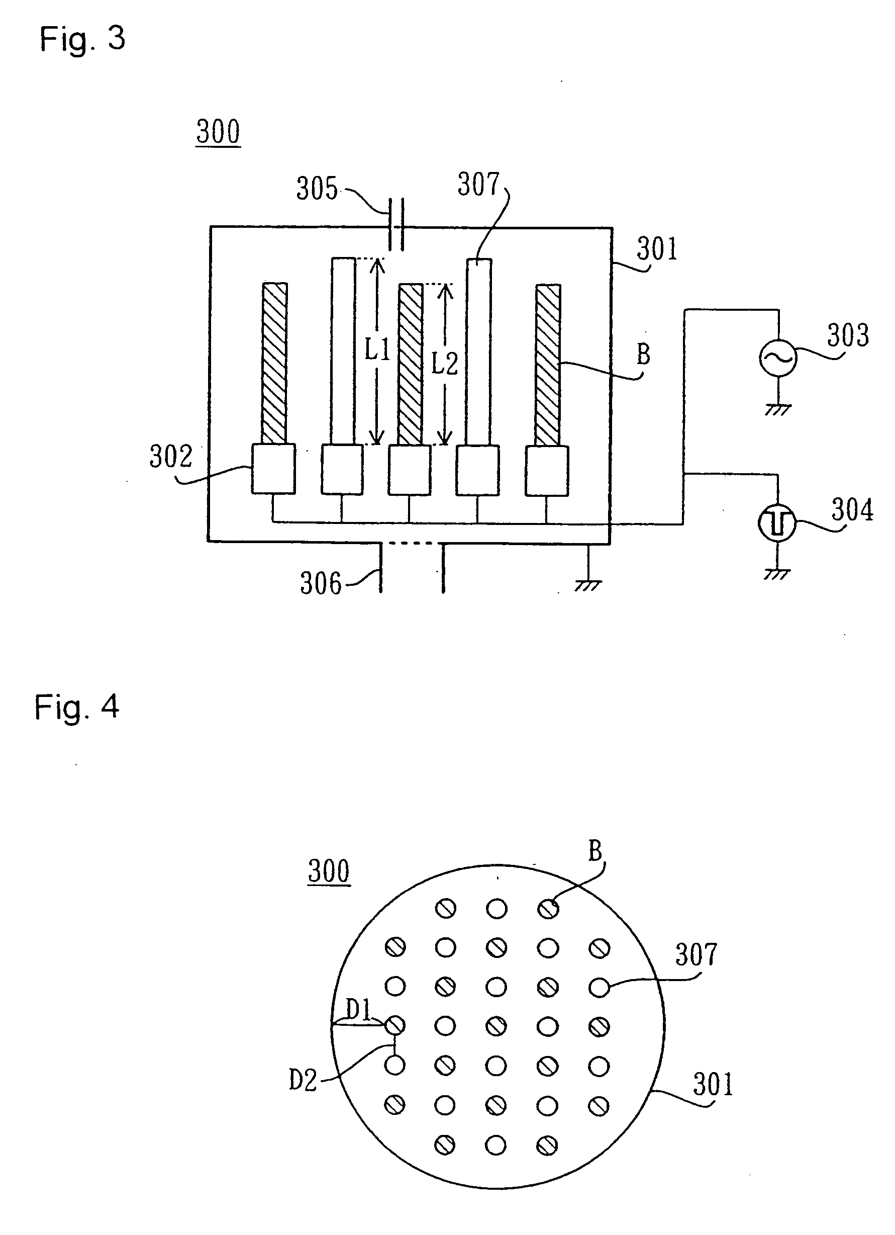
[0064]FIG. 11 is an outline of an example of a CVD deposition apparatus used when implementing the method for deposition onto a substrate related to the second embodiment of the present invention. FIG. 12 shows a view from above the inside of the vacuum container of the CVD deposition apparatus shown in FIG. 11.

[0065] The CVD deposition apparatus 1100 shown in FIG. 11 differs from the CVD deposition apparatus 300 shown in FIG. 3 by the fact that ground members 1101 are enclosed at the inside of the substrates B. According to the CVD deposition apparatus 1100 related to the second embodiment, the space required for the ground members 307 which require independent space can be reduced compared to the CVD deposition apparatus 300 related to the first embodiment. Therefore, this CVD deposition apparatus 1100 is suitable when manufacturing a greater quantity of photosensitive material.

[0066] As shown in FIG. 12, the ground members 1101 have a hollow cylindrical shape. The substrates B ...

third embodiment

[0074] The method for deposition onto a substrate related to the third embodiment differs from the method for deposition onto a substrate related to the second embodiment by the fact that the gas pressure while plasma generates in proportion to the distance between the substrates B and the ground members 1101 as well as the high-frequency output to the substrates B in the CVD deposition apparatus 1100 related to the second embodiment are both controlled. By controlling the gas pressure while plasma generates in proportion to the distance between the substrates B and the ground members 1101 in this manner makes it possible to optimize the state of the plasma around the periphery of the substrates B and to also optimize the deposition of coatings onto the substrates B.

[0075]FIG. 14 shows an example of a Paschen curve utilized when the method for deposition onto a substrate related to the third embodiment controls the gas pressure while plasma generates in proportion to the distance (...


PUM

PropertyMeasurementUnit
Thicknessaaaaaaaaaa
Thicknessaaaaaaaaaa
Pressureaaaaaaaaaa

Abstract

A grounded vacuum container is filled, the container containing a plurality of substrates, with a CVD gas. A voltage is applied to the substrates to generate plasma around each of the substrates along with grounding a plurality of ground members arranged at positions opposite to the deposition surface of each of the substrates inside the vacuum container. A coating is deposited onto a plurality of substrates in a method for deposition that attracts ions within the plasma to the substrates and deposits a coating onto the substrates.

Description

BACKGROUND OF THE INVENTION [0001] 1. Field of the Invention [0002] The present invention relates to a method for deposition onto a substrate and a method for producing a photo conductor. These are utilized for, for example, a photo conductor used in electrophotographic copying machines and printers. [0003] 2. Description of Related Art [0004] Conventional plasma CVD methods are known that change the raw gas used for the deposition into plasma by applying high-frequency electric power or a high-power voltage pulse and high-frequency electric power, expose substrates to this plasma, and then deposit a coating onto the substrate. (As an example refer to Related Art 1 and Related Art 2.) [0005] Furthermore, manufacturing methods of the photo conductor used in electrophotography which use plasma CVD methods are also known. This photo conductor is comprised by an optically conductive layer that includes an amorphous crystal material with a base material of silicon atoms or a protective s...

Claims


Application Information

Patent Timeline
IPC IPC(8): C23C8/00
CPCC23C16/509H01J37/32706H01L31/08H01L31/1804Y02P70/50
Inventor KURAMOTO, YUKIMASATAKIMOTO, SATOSHISHINGAE, RYUICHI
Owner PANASONIC CORP
Why Eureka
Try Eureka