Dual detector optics for simultaneous collection of secondary and backscattered electrons

a detector optics and electron detector technology, applied in the field of electron detector optics, can solve the problems of inability to fully separate se and bse signals, cost, undesirable fluctuations, etc., and achieve the effect of reducing cost and complexity

Active Publication Date: 2006-03-16
MULTIBEAM CORP
View PDF16 Cites 23 Cited by
  • Summary
  • Abstract
  • Description
  • Claims
  • Application Information

AI Technical Summary

Benefits of technology

[0021] Another aspect of the present invention is a detector optics electrode configuration which avoids almost all interaction between the primary electron beam and the electric fields due to the SE and BSE detectors. This is accomplished in a much simpler way than for the case of Wien filter detectors, thereby reducing cost and complexity.

Problems solved by technology

These fluctuations are undesirable since they cannot be distinguished from fluctuations arising from surface topography, elemental composition variations or changes in the surface voltage.
There are several limitations to this approach: 1) Cost—a Wien filter requires complex machining of magnetic and electrode materials, as well as power supplies for the magnet coils.
2) Aberrations—the Wien filter always introduces some aberration (particularly chromatic) into the primary beam—this is a problem in low-voltage columns where the fractional energy spread (=ΔV / V0, where ΔV=the energy spread and V0=the column accelerating voltage) is larger.
3) Coupling between the SE and BSE signals—in many cases it is not possible to fully separate the SE and BSE signals, i.e., some of the SEs are collected by the BSE detector and some of the BSEs are collected by the SE detector.
This requirement typically limits the detector collection efficiencies.

Method used


Image

  • Dual detector optics for simultaneous collection of secondary and backscattered electrons
  • Dual detector optics for simultaneous collection of secondary and backscattered electrons
  • Dual detector optics for simultaneous collection of secondary and backscattered electrons

Examples


Embodiment Construction

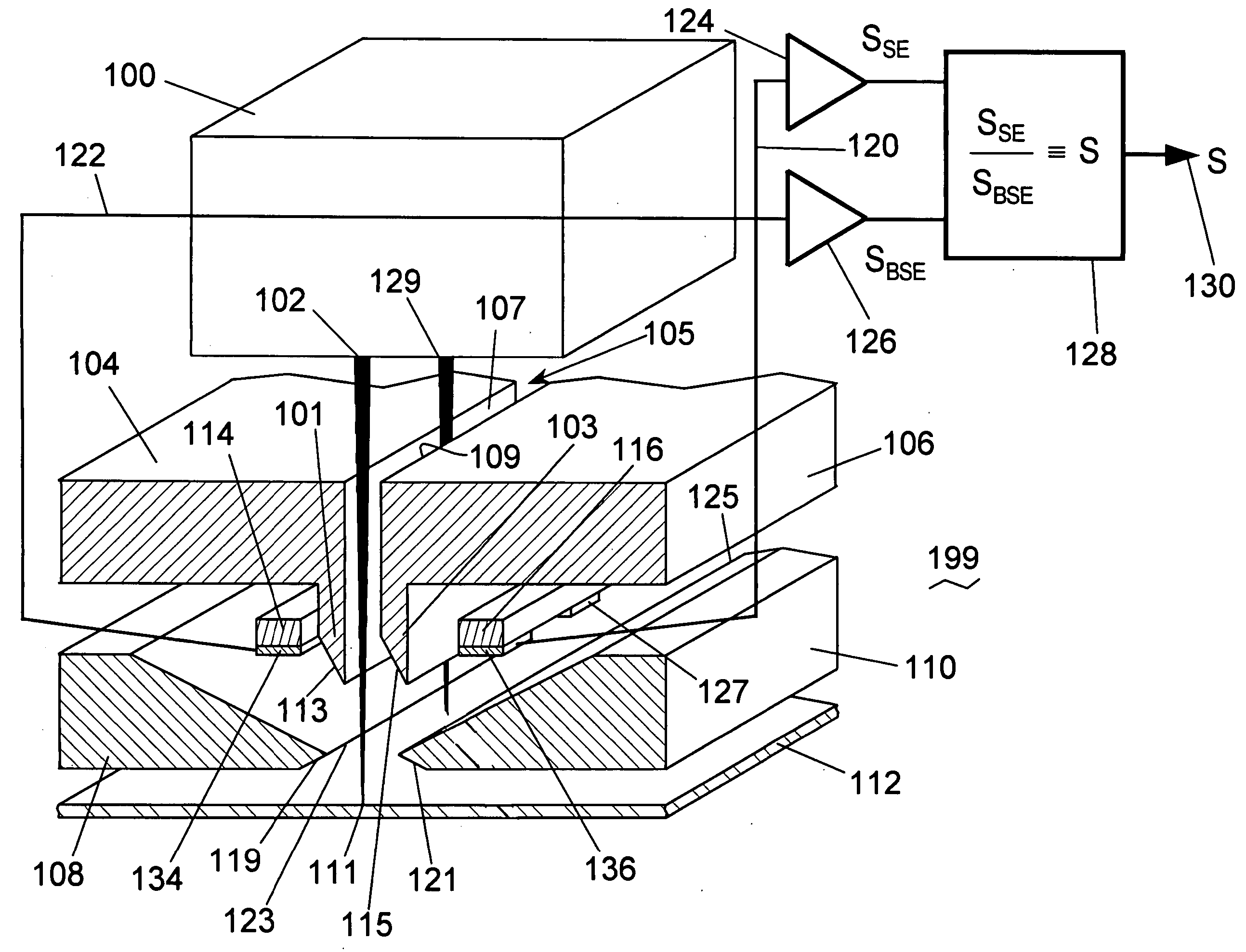
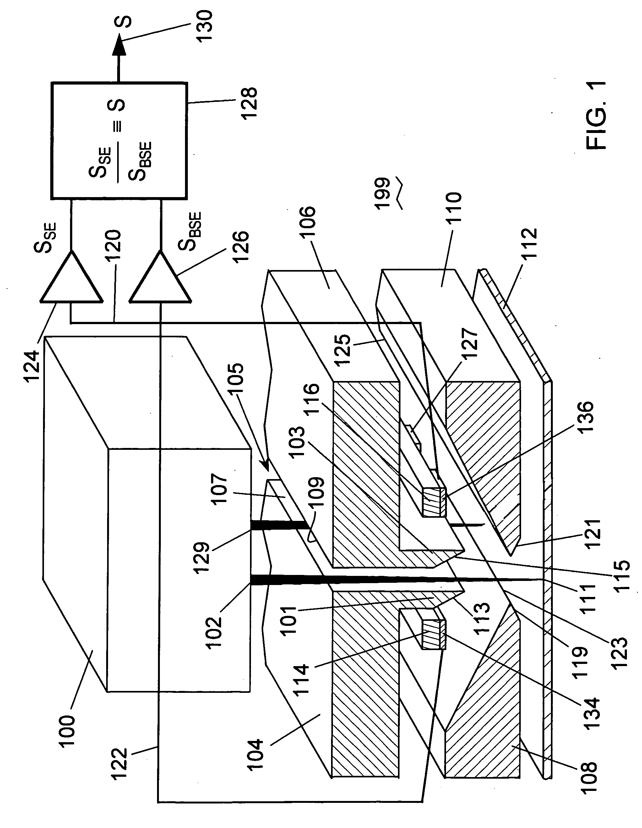
[0050] The present invention disclosed herein is a detector optics system having dual detectors, one with high secondary electron (SE) detection efficiency combined with minimal resultant distortion of the electron beam, and the other for simultaneous detection of backscattered electrons (BSEs). The various detector optics electrodes are designed to make the secondary electron detection efficiency a nearly linearly-varying monotonic function of the substrate surface voltage, while the backscattered electron detection efficiency remains independent of the substrate surface voltage. Both the SE and BSE signals are proportional to the current in the primary electron beam which induces the emission of both the SEs and BSEs. The ratio of the SE and BSE signals, however, is independent of the current in the primary electron beam and is also a rapidly-varying monotonic function of the substrate surface voltage, enabling surface voltage measurements to be made at high bandwidth without fluc...


PUM

PropertyMeasurementUnit
energyaaaaaaaaaa
energyaaaaaaaaaa
emission anglesaaaaaaaaaa

Abstract

A detector optics system for an electron probe system is disclosed. Aspects of the detector optics system include: the ability to simultaneously detect two electron populations, secondary electrons (SEs) and backscattered electrons (BSEs), wherein both populations are emitted from a substrate due to the impact of the electron probe. The design of the detector optics utilizes a field-free tunnel and substrate electric-field control electrodes to enable separation of the SEs and BSEs into two detectors, allowing simultaneous acquisition of topographic and elemental composition data, with minimal impact on the electron probe. The secondary electron signal is a monotonically-varying function of the voltage on the substrate surface. The ratio of the SE signal to the BSE signal gives a testing signal which is independent of the primary beam current and serves as an absolute voltage probe of surface voltages without the need for an external reference voltage.

Description

CROSS-REFERENCE TO RELATED APPLICATIONS [0001] This application claims the benefit of U.S. provisional application Ser. No. 60 / 608,609 filed Sep. 10, 2004.BACKGROUND OF THE INVENTION [0002] 1. Field of the Invention [0003] This invention relates generally to the field of electron optics, and more particularly to electron detector optics for large substrate electron-beam testing systems. [0004] 2. Description of the Related Art [0005] Electron beam systems employed for testing or inspection purposes typically generate a primary electron beam (or “probe”) which is focused onto the surface of a substrate by probe-forming optics. The signal detection process generally involves the collection of secondary electrons (SEs) and / or backscattered electrons (BSEs) which are emitted from the substrate surface as a result of the interaction of the primary electron beam with the substrate surface. In LCD substrate testing systems, the energy of the primary electron beam striking the substrate sur...

Claims


Application Information

Patent Timeline
Patent Type & Authority Applications(United States)
IPC IPC(8): H01J37/28G01N23/225H01J37/244
CPCH01J37/244H01J2237/2448H01J2237/24475H01J2237/0492
Inventor PARKER, N. WILLIAM
Owner MULTIBEAM CORP
Why Eureka
Try Eureka