Method of driving liquid crystal display device and liquid crystal display device

a technology of liquid crystal display device and display device, which is applied in the field of driving a liquid crystal display device, can solve the problems of capacitive coupling, the phenomenon of whitish screen, and the variation of the contrast or color tone of the screen, so as to avoid a rise in the cost of manufacturing and avoid the effect of rising the cost of manufacturing

Inactive Publication Date: 2006-03-16
SHARP KK
View PDF45 Cites 20 Cited by
  • Summary
  • Abstract
  • Description
  • Claims
  • Application Information

AI Technical Summary

Benefits of technology

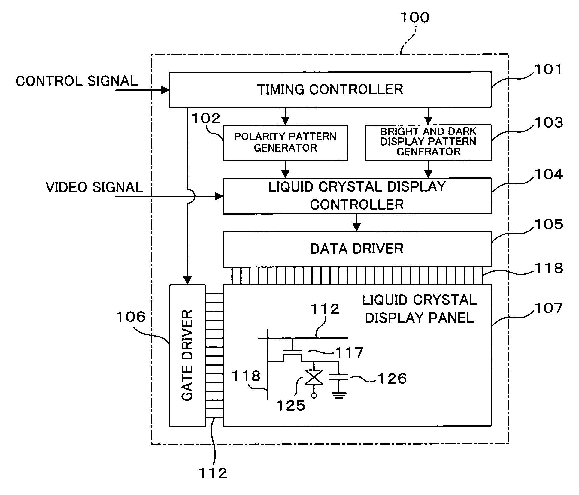
[0054] Currently, almost all of driver ICs (integrated circuits) in general use are adapted either to apply voltages of opposite polarities to adjacent data bus lines or to apply a voltage of the same polarity to all data bus lines. In the invention, two data drivers are used. One data driver is used to control the polarity of a display signal to be fed to an odd-numbered data bus line, and the other data driver is used to control the polarity of a display signal to be fed to an even-numbered data bus line. The above-described driving method, which is implemented by using these data drivers to control the polarity of the display signal, permits the use of any general-purpose driver IC, thus avoiding a rise in the cost of manufacturing the liquid crystal display device.
[0055] Moreover, the liquid crystal display device includes the wiring replacement part which feeds signals, which are outputted through the (4k+1)th, (4k+2)th, (4k+3)th, and (4k+4)th output terminals of the data driver, to the (4k+1)th, (4k+3)th, (4k+2)th, and (4k+4)th data bus lines, respectively. This permits the use of any general-purpose driver IC, thus avoiding a rise in the cost of manufacturing the liquid crystal display device.

Problems solved by technology

However, the TN liquid crystal display device has the disadvantage of having poor viewing angle characteristics and thus causing considerable variations in the contrast or color tone of a screen as viewed from any oblique angle.
When the screen is viewed from the oblique angle, such low transmittance leads to small luminance differences among red, green and blue picture elements, thus resulting in the occurrence of the phenomenon in which the screen becomes whitish, as mentioned above.
The HT technique based on capacitive coupling has the disadvantage of reducing an aperture ratio and thus providing insufficient brightness, because a voltage to be applied to each sub picture element electrode cannot be used to provide a desired orientation of liquid crystal molecules in a region between the sub picture element electrodes.
This HT technique also has the disadvantage of increasing the likelihood of a short circuit occurring between the sub picture element electrodes and the control electrodes or between adjacent sub picture element electrodes, because of requiring a thin insulating film between the control electrodes and the picture element electrodes or a slit of narrow width between the sub picture element electrodes.
However, experimental tests and research carried out by the inventors have shown that the technique disclosed in the publication No. 2001-75073, as applied to MVA liquid crystal display devices, cannot achieve its full effect.
In other words, the HT technique based on time division cannot achieve its effect and thus improve viewing angle characteristics, when the difference between the voltages V1 and V2 is such that the luminance difference is unnoticeable as described in the publication No. 2001-75073.
Such a large difference between the voltages V1 and V2 causes a severe flicker in full screen, when the bright and dark display patterns shown in FIGS. 7A and 7B are used to drive the liquid crystal display panel.
In short, the technique disclosed in the publication No. 2001-75073 has at least three problems as given below: (1) an input signal does not match output brightness; (2) the technique does not achieve the effect of improving viewing angle characteristics, when there is little gray level difference; and (3) the bright and dark display pattern is noticeable, when there is a large gray level difference.
This leads to the application of a direct-current component to a liquid crystal layer, and thus results in the occurrence of burn-in or flicker.
Thus, a considerable imbalance in electric potential in the picture elements connected to one gate bus line, as shown in FIGS. 13E and 13F, causes variations in the electric potentials of the gate bus line and the auxiliary capacitance bus line.
This causes flicker in each transverse line.
However, the approach shown in FIGS. 14A to 14F has the disadvantage of producing a coarse screen, because of changing bright display and dark display every two horizontal picture elements.

Method used


Image

  • Method of driving liquid crystal display device and liquid crystal display device
  • Method of driving liquid crystal display device and liquid crystal display device
  • Method of driving liquid crystal display device and liquid crystal display device

Examples


first modified embodiment

[First Modified Embodiment]

[0115] A driver IC (integrated circuit), which is adapted to reverse the polarity every two data bus lines 118, is necessary in order to implement a driving method as shown in FIGS. 20A to 20D. However, almost all of driver ICs in current use are adapted either to apply voltages of opposite polarities to adjacent data bus lines or to apply a voltage of the same polarity to all data bus lines. A driver IC may be newly designed to generate the polarity patterns as shown in FIGS. 20A to 20D. In this case, the driver IC, however, cannot be used for general purposes, and thus leads to a rise in the cost of manufacturing the liquid crystal display device.

[0116] A first modified embodiment uses a general-purpose driver IC which is conventionally used. Specifically, driver ICs 151 and 152 are disposed over and under the liquid crystal display panel 107, respectively, as shown in FIG. 21. The upper driver IC 151 is used to drive odd-numbered data bus lines 118, an...

second modified embodiment

[0118]FIG. 22 is a schematic illustration showing a liquid crystal display device according to a second modified embodiment. In the second modified embodiment, a general-purpose driver IC 153 is also used. In the second modified embodiment, the horizontally arranged data bus lines 118 are divided into groups of four, starting at the leftmost end. The second ((4k+2)th) data bus line 118 from the left, which belongs to each group, crosses and is connected to the third ((4k+3)th) metal wiring 161 (where k denotes any natural number including 0). More specifically, the (4k+1)th, (4k+2)th, (4k+3)th, and (4k+4)th metal wirings 161 are connected to the (4k+1)th, (4k+3)th, (4k+2)th, and (4k+4)th data bus lines 118, respectively. When the metal wirings arranged in sequence are connected to the data bus lines arranged in sequence, the metal wiring and the data bus line having different numbers are connected as mentioned above. Hereinafter, this connection is referred to as “wiring replacement...


PUM


Abstract

A combination of a bright and dark display pattern and a polarity pattern is used to drive a liquid crystal display device. In the bright and dark display pattern, bright display picture elements and dark display picture elements alternate with each other every one picture element in horizontal and vertical directions. In the polarity pattern, positive-polarity picture elements and negative-polarity picture elements alternate with each other every two picture elements in the horizontal and vertical directions. This driving method allows preventing a phenomenon in which a screen becomes whitish when viewed from any oblique angle (i.e., washing out), that is, what the effect of HT technique based on time division is aiming at, while preventing the occurrence of flicker and burn-in on the screen. Moreover, the driving method enables coarseness-free excellent display, because the bright display picture elements and the dark display picture elements alternate with each other every one picture element.

Description

CROSS-REFERENCE TO RELATED APLICATIONS [0001] This application is based on and claims priority of Japanese Patent Application No. 2004-270308 filed on Sep. 16, 2004, the entire contents of which are incorporated herein by reference. BACKGROUND OF THE INVENTION [0002] 1. Field of the Invention [0003] The invention relates to a method of driving a liquid crystal display device and a liquid crystal display device, which are adapted to change, with time, the gray level of a display signal to be fed to each picture element of a liquid crystal display panel, thereby preventing the occurrence of a phenomenon in which an image as viewed from any oblique angle undergoes degradation in its color reproducibility, as compared to that as viewed from the front. [0004] 2. Description of the Prior Art [0005] Liquid crystal display devices have the advantages of being thin and lightweight and also allowing low-voltage drive and thus low power consumption, as compared to CRTs (cathode ray tubes). Thu...

Claims


Application Information

Patent Timeline
Patent Type & Authority Applications(United States)
IPC IPC(8): G09G3/36
CPCG02F1/13452G02F1/136213G02F2001/13629G02F2203/30G09G2330/08G09G3/3648G09G2310/0218G09G2320/028G09G3/3614G02F1/13629A61F7/007A61F7/08A61G13/009A61H1/005A61H1/0218A61H2201/0142A61H2201/10A61H2201/1642A61N2005/066
Inventor KAMADA, TSUYOSHIYOSHIDA, HIDEFUMISHIBASAKI, MASAKAZUSUZUKI, TOSHIAKI
Owner SHARP KK
Why Eureka
Try Eureka