Semiconductor light source with electrically tunable emission wavelength

a semiconductor and light source technology, applied in semiconductor lasers, laser details, electrical equipment, etc., can solve the problems of difficult laser wavelength tuning, serious drawbacks of suggested schemes, and inability to control the generation wavelength

Inactive Publication Date: 2006-03-16
MAXION TECH +1
View PDF8 Cites 54 Cited by
  • Summary
  • Abstract
  • Description
  • Claims
  • Application Information

AI Technical Summary

Problems solved by technology

However, the suggested schemes have serious drawbacks.
This makes it difficult to use such designs for laser wavelength tuning since the carrier concentration in the emitter is pinned after the laser generation onset, and generation wavelength cannot be controlled through the Stark shift unless a controlled optical loss is introduced in the laser cavity.

Method used


Image

  • Semiconductor light source with electrically tunable emission wavelength
  • Semiconductor light source with electrically tunable emission wavelength
  • Semiconductor light source with electrically tunable emission wavelength

Examples


Embodiment Construction

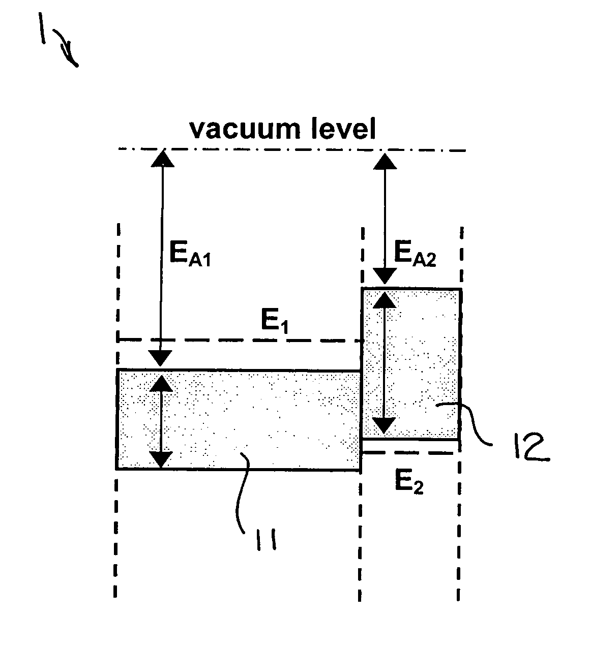
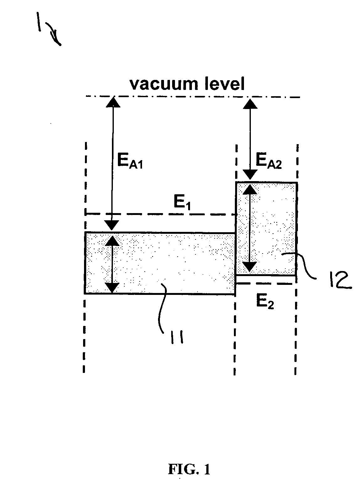
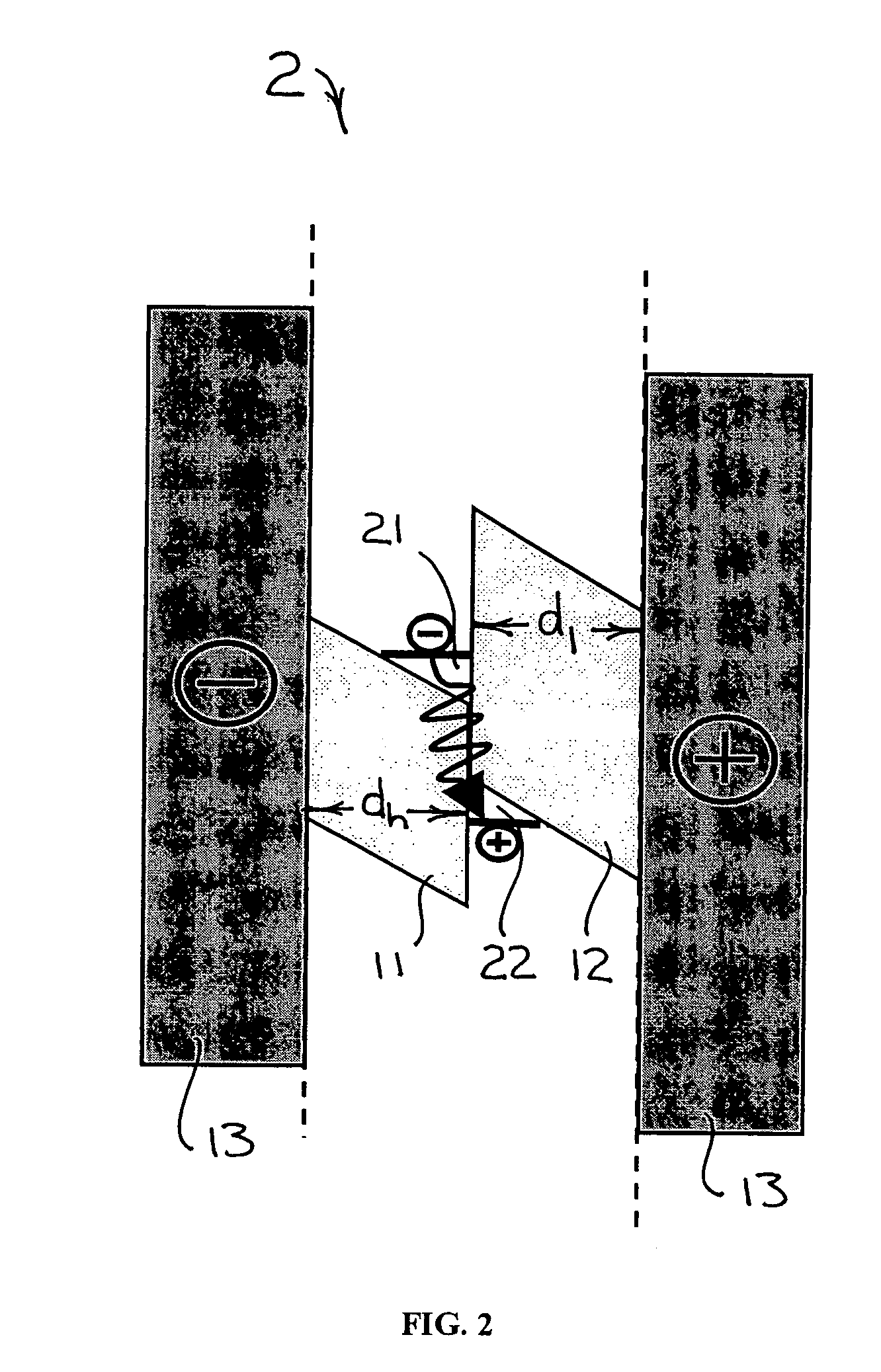
[0033] The present semiconductor structures include a tunable semiconductor light source having an emission wavelength which may be electrically tunable in a wide range. FIG. 1 shows one period of the active region of a semiconductor light source 1 in accordance with an embodiment of the present invention. The semiconductor light source has an electrically tunable emission wavelength provided by two semiconductor layers, 11 and 12, with type-II band alignment. Layer 11 is characterized by higher electron affinity, and layer 12 is characterized by lower electron affinity. As used herein, the terms “higher” and “lower” electron affinity are relative to each other.

[0034] The purpose of the active region is to form energy levels E1 and E2 for the optical transition. The radiation wavelength λ is related to the energy separation E=E1−E2:

λ=hc / E,

where h is the Planck constant and c is the light velocity in vacuum. The active region comprises two layers of semiconductor materials with e...


PUM


Abstract

A semiconductor light source is disclosed comprising a substrate, lower and upper claddings, a waveguide region with imbedded active area, and electrical contacts to provide voltage necessary for the wavelength tuning. The active region includes single or several heterojunction periods sandwiched between charge accumulation layers. Each of the active region periods comprises higher and lower affinity semiconductor layers with type-II band alignment. The charge carrier accumulation in the charge accumulation layers results in electric field build-up and leads to the formation of generally triangular electron and hole potential wells in the higher and lower affinity layers. Nonequillibrium carriers can be created in the active region by means of electrical injection or optical pumping. Radiative recombination occurs between the electrons and holes, accumulated in the ground states of the triangular potential wells formed in the high- and low-affinity layers of each active region periods. The ground state energy in the triangular wells and the radiation wavelength can be tuned by changing the voltage drop across the active region.

Description

CROSS-REFERENCE TO RELATED APPLICATIONS [0001] This application claims the benefit of U.S. Provisional Patent Application Ser. No. 60 / 602,750 filed Aug. 19, 2004, which is incorporated herein by reference.GOVERNMENT CONTRACT [0002] The present invention was supported by the United States Air Force Research Laboratory under Contract No. F19628-02-C-0032 and by the United States Department of Energy under Contract No. DE-FG02-02ER83492. The present invention was also supported by ARO Grant No. DAAD190310259 and AFOSR Grant No. F49620-00-1-0331. The United States Government has certain rights in this invention.FIELD OF THE INVENTION [0003] This invention relates generally to the field of tunable semiconductor electromagnetic radiation sources and, in particular, to an electrically tunable semiconductor source of electromagnetic radiation. BACKGROUND INFORMATION [0004] Tunable semiconductor light sources such as lasers and light diodes are in high demand for various applications such as...

Claims


Application Information

Patent Timeline
Patent Type & Authority Applications(United States)
IPC IPC(8): H01S3/10
CPCB82Y20/00H01S5/0622H01S5/3422H01S5/3402H01S5/3401H01S5/322
Inventor BELENKY, GREGORYBRUNO, JOHN D.KISIN, MIKHAIL V.LURYI, SERGESHTERENGAS, LEONSUCHALKIN, SERGEYTOBER, RICHARD L.
Owner MAXION TECH
Why Eureka
Try Eureka