Method and apparatus for manufacturing display

Active Publication Date: 2006-03-16
JAPAN DISPLAY CENT INC
View PDF2 Cites 35 Cited by
  • Summary
  • Abstract
  • Description
  • Claims
  • Application Information

AI Technical Summary

Benefits of technology

[0013] It is an object of the present invention to accurately control the substrate temperature when film format

Problems solved by technology

The existence of water significantly shortens the lifetime of the organic EL element.
This makes it difficult to well cool the insulating substrate before the formation of the organic layer is started.
Also, in a film formation method such as vacuum evaporation or sputtering, it is originally unnecessary to heat a substrate on which a layer is to be formed.
Accordingly, especially when a multilayered structure is used as an organic layer or a plurality of typ

Method used


Image

  • Method and apparatus for manufacturing display
  • Method and apparatus for manufacturing display
  • Method and apparatus for manufacturing display

Examples


Embodiment Construction

[0027] An embodiment of the present invention will be described in detail below with reference to the accompanying drawing. Note that in the drawing, the same reference numerals denote constituent elements having the same or similar functions, and a repetitive explanation thereof will be omitted.

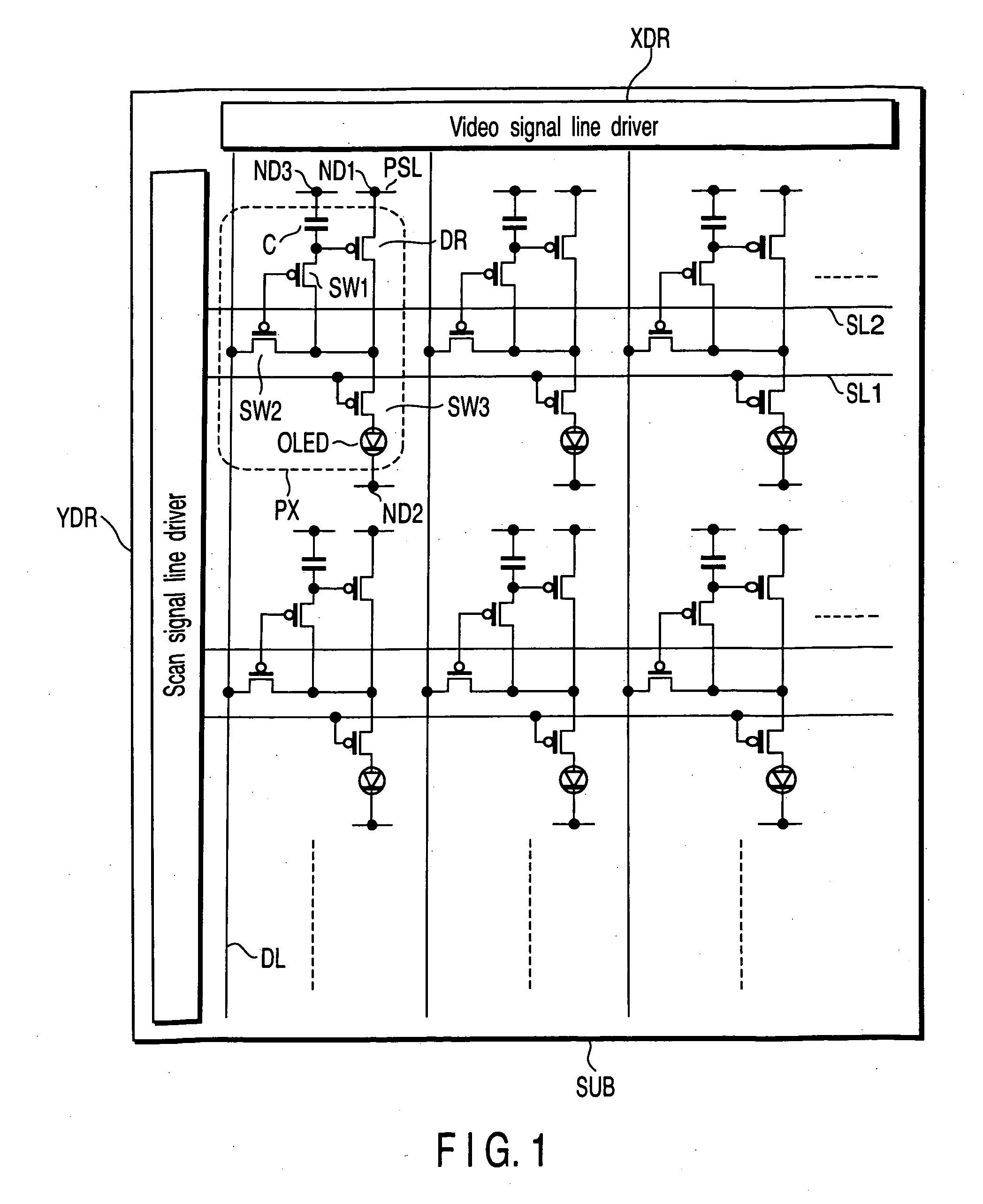
[0028]FIG. 1 is a plan view schematically showing an example of a display which can be manufactured by a method according to an embodiment of the present invention. That is, FIG. 1 shows an active matrix organic EL display as an example.

[0029] This organic EL display includes a plurality of pixels PX. The pixels PX are arranged in a matrix form on an insulating substrate SUB such as a glass substrate.

[0030] On the substrate SUB, a scan signal line driver YDR and video signal line driver XDR are also arranged.

[0031] On the substrate SUB, scan signal lines SL1 and SL2 connected to the scan signal line driver YDR run in the row direction of the matrix of pixels PX. The scan signal line driv...


PUM


Abstract

Provided is a method of manufacturing a display which includes an insulating substrate and a structure formed on the insulating substrate and including a display element, including forming a patterned layer as a portion of the structure on the insulating substrate by vapor deposition in vacuum using a mask, and cooling the insulating substrate before and/or during formation of the patterned layer by arranging a cooling plate which comprises a metal substrate and an infrared absorption layer covering a main surface of the metal substrate and being larger in infrared absorptance than the metal plate such that the infrared absorption layer faces the insulating substrate.

Description

CROSS-REFERENCE TO RELATED APPLICATIONS [0001] This application is based upon and claims the benefit of priority from prior Japanese Patent Application No. 2004-267021, filed Sep. 14, 2004, the entire contents of which are incorporated herein by reference. BACKGROUND OF THE INVENTION [0002] 1. Field of the Invention [0003] The present invention relates to a method and apparatus for manufacturing a display and, more particularly, to a method and apparatus for manufacturing a display whose manufacturing process includes forming a patterned layer on an insulating substrate by vapor deposition in vacuum using a mask. [0004] 2. Description of the Related Art [0005] In the manufacture of a flat panel display, a patterned layer is sometimes formed on an insulating substrate by vapor deposition in vacuum using a mask. For example, in the manufacture of an organic electroluminescent (EL) display, an organic layer of an organic EL element is sometimes formed by vacuum evaporation using a mask...

Claims


Application Information

Patent Timeline
IPC IPC(8): H01L29/74H01L27/10H01L21/00
CPCH01L29/78603H01L27/1214H01L27/1259H05B33/10
Inventor AOKI, MOTONOBUISHIDA, TETSUO
Owner JAPAN DISPLAY CENT INC
Why Eureka
Try Eureka