[0010] In consideration of such a problem of the related art, the present invention intends to provide a pixel circuit, a display, and a driving method thereof that each allows simultaneous correction of influence of both the
threshold voltage and mobility, to thereby permit compensation of variation in the
drain current (output current) supplied from the drive transistor. To this end, the following configuration is implemented. Specifically, according to an embodiment of the invention, there is provided a pixel circuit disposed at an intersection between a row
scan line that supplies a control pulse and a column
signal line that supplies a video
signal. The pixel circuit includes a sampling transistor conducting in response to the control pulse supplied from the
scan line to sample the video
signal supplied from the signal line during a certain sampling period, a capacitance part holding an input potential dependent upon the sampled video signal, and a drive transistor supplying an output current during a certain emission period according to the input potential held by the capacitance part. The output current has dependence on a carrier mobility in a channel region of the drive transistor and dependence on a threshold
voltage of the drive transistor. The pixel circuit also includes a light-emitting element caused, by the output current supplied from the drive transistor, to emit light with a luminance in response to the video signal, and correction means correcting both the dependence of the output current on the carrier mobility and the dependence of the output current on the threshold
voltage simultaneously. The correction section is connected to the drive transistor and the capacitance part, and operates during a correction period preceding to the sampling period. The correction period is separated into a reset period and a detection period. During the reset period, the correction section energizes the capacitance part to reset the potential held by the capacitance part. During the detection period, the correction section stops the energization and detects a
potential difference arising between a source and a gate of the drive transistor during a period when a
transient current flows through the drive transistor. The capacitance part holds a potential corresponding to the detected potential difference. The held potential includes both a potential component for reducing influence of the threshold
voltage on the output current of the drive transistor, and a potential component for reducing influence of the carrier mobility on the output current of the drive transistor.
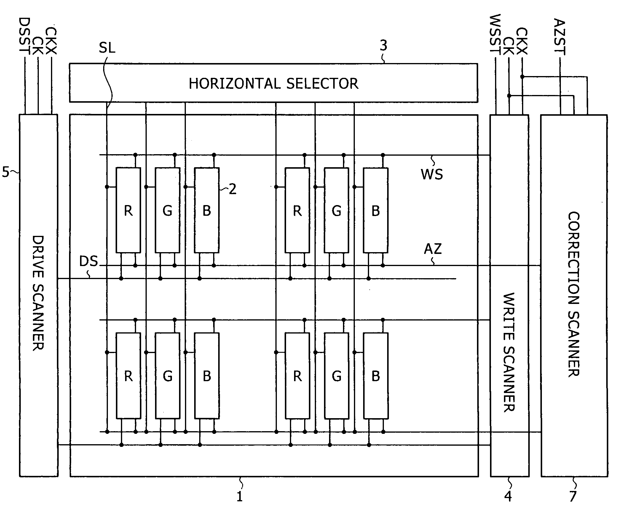
[0011] Furthermore, according to an embodiment of the invention, there is provided a display that includes a
pixel array part having scan lines disposed on rows,
signal lines disposed on columns, and a matrix of pixels disposed at intersections between the scan and
signal lines, a signal part supplying a video signal to the
signal lines, and a
scanner part supplying a control pulse to the scan lines to sequentially scan the pixels for each row. Each of the pixels includes at least a sampling transistor, a capacitance part, a drive transistor, and a light-emitting element. The sampling transistor conducts in response to a sampling control pulse supplied from the
scan line to sample the video signal supplied from the signal line during a certain sampling period. The capacitance part holds an input potential dependent upon the sampled video signal. The drive transistor supplies an output current during a certain emission period according to the input potential held by the capacitance part. The output current has dependence on a carrier mobility in a channel region of the drive transistor and dependence on a threshold voltage of the drive transistor. The light-emitting element is caused, by the output current supplied from the drive transistor, to emit light with a luminance in response to the video signal. Each of the pixels includes correction means that corrects both the dependence of the output current on the carrier mobility and the dependence of the output current on the threshold voltage simultaneously. The correction section is connected to the drive transistor and the capacitance part, and operates during a correction period preceding to the sampling period. The correction period is separated into a reset period and a detection period. During the reset period, the correction section energizes the capacitance part to reset the potential held by the capacitance part. During the detection period, the correction section stops the energization and detects a potential difference arising between a source and a gate of the drive transistor during a period when a
transient current flows through the drive transistor. The capacitance part holds a potential corresponding to the detected potential difference. The held potential includes both a potential component for reducing influence of the threshold voltage on the output current of the drive transistor, and a potential component for reducing influence of the carrier mobility on the output current of the drive transistor. The
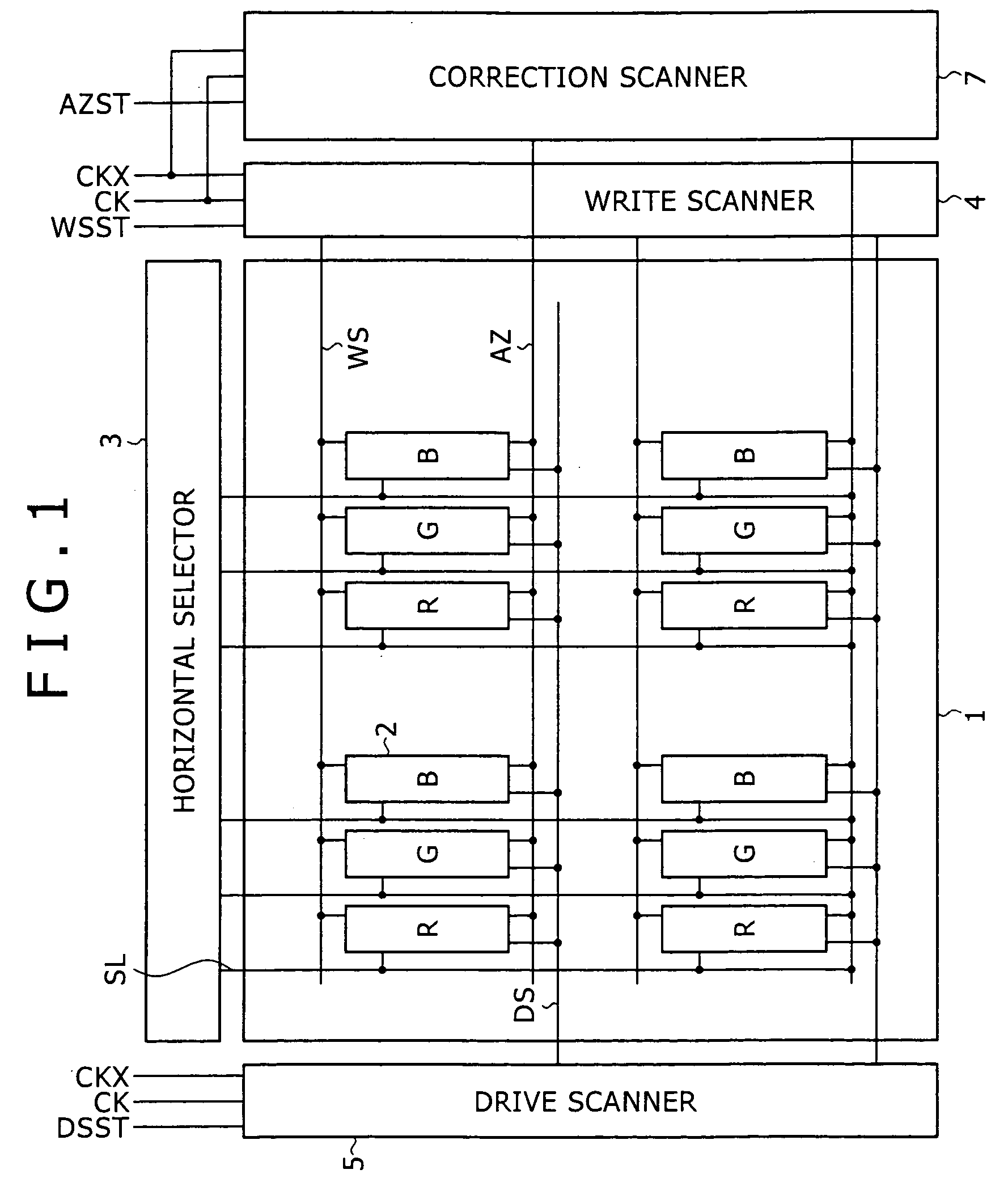
scanner part includes at least a write
scanner, a drive scanner, and a correction scanner. The write scanner supplies the sampling control pulse to the scan lines during the sampling period. The correction scanner supplies a correction control pulse that defines the correction period to the scan lines. The drive scanner supplies a drive control pulse to the scan lines. The drive control pulse differentiates the reset period from the detection period in the correction period and differentiates an emission period from a non-emission period other than the emission period.
[0012] Moreover, according to an embodiment of the invention, there is provided a method of driving a pixel circuit disposed at an intersection between a row scan line that supplies a control pulse and a column signal line that supplies a video signal. The pixel circuit includes at least a sampling transistor, a capacitance part, a drive transistor and a light-emitting element. The sampling transistor conducts in response to the control pulse supplied from the scan line to sample the video signal supplied from the signal line during a certain sampling period. The capacitance part holds an input potential dependent upon the sampled video signal. The drive transistor supplies an output current during a certain emission period according to the input potential held by the capacitance part. The output current has dependence on a carrier mobility in a channel region of the drive transistor and dependence on a threshold voltage of the drive transistor. The light-emitting element is caused, by the output current supplied from the drive transistor, to emit light with a luminance in response to the video signal. The method includes a correction step for correcting both the dependence of the output current on the carrier mobility and the dependence of the output current on the threshold voltage simultaneously during a correction period preceding to the sampling period. The correction period is separated into a reset period and a detection period. The correction step includes the sub steps of: energizing the capacitance part to reset the potential held by the capacitance part during the reset period; and stopping the energization and detecting a potential difference arising between a source and a gate of the drive transistor during a period when a transient current flows through the drive transistor during the detection period. The method also includes a holding step for holding a potential corresponding to the detected potential difference in the capacitance part. The held potential includes both a potential component for reducing influence of the threshold voltage on the output current of the drive transistor, and a potential component for reducing influence of the carrier mobility on the output current of the drive transistor.
[0013] In addition, according to an embodiment of the invention, there is provided a method of driving a display including a
pixel array part, a scanner part and a signal part. The
pixel array part includes scan lines disposed on rows, signal lines disposed on columns, and a matrix of pixels disposed at intersections between the scan and signal lines. The signal part supplies a video signal to the signal lines. The scanner part supplies a control pulse to the scan lines to sequentially scan the pixels for each row. Each of the pixels includes at least a sampling transistor, a capacitance part, a drive transistor and a light-emitting element. The sampling transistor conducts in response to a sampling control pulse supplied from the scan line to sample the video signal supplied from the signal line during a certain sampling period. The capacitance part holds an input potential dependent upon the sampled video signal. The drive transistor supplies an output current during a certain emission period according to the input potential held by the capacitance part. The output current has dependence on a carrier mobility in a channel region of the drive transistor and dependence on a threshold voltage of the drive transistor. The light-emitting element is caused, by the output current supplied from the drive transistor, to emit light with a luminance in response to the video signal. The method includes a correction step for correcting at each pixel both the dependence of the output current on the carrier mobility and the dependence of the output current on the threshold voltage simultaneously during a correction period preceding to the sampling period. The correction period is separated into a reset period and a detection period. The correction step includes the sub steps of: energizing the capacitance part to reset the potential held by the capacitance part during the reset period; and stopping the energization and detecting a potential difference arising between a source and a gate of the drive transistor during a period when a transient current flows through the drive transistor during the detection period. The method also includes a holding step for holding a potential corresponding to the detected potential difference in the capacitance part. The held potential includes both a potential component for reducing influence of the threshold voltage on the output current of the drive transistor, and a potential component for reducing influence of the carrier mobility on the output current of the drive transistor. The method further includes a write scanning step for supplying the sampling control pulse to the scan lines during the sampling period, a correction scanning step for supplying a correction control pulse that defines the correction period to the scan lines, and a drive scanning step for supplying a drive control pulse to the scan lines. The drive control pulse differentiates the reset period from the detection period in the correction period and differentiates an emission period from a non-emission period other than the emission period.
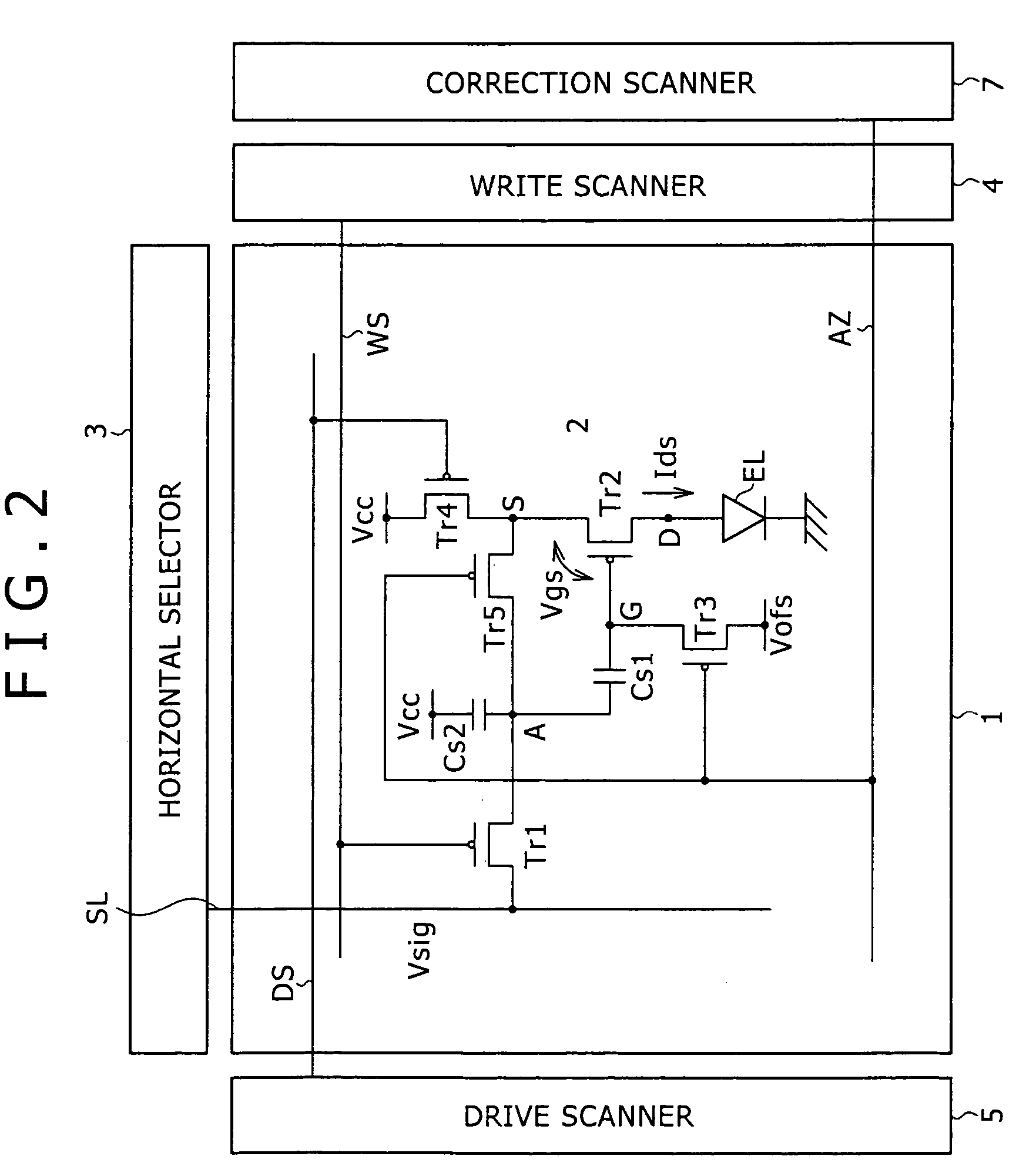
[0014] According to an embodiment of the invention, the pixel circuit corrects both the dependence of the output current on the carrier mobility and that on the threshold voltage simultaneously. Specifically, in a certain detection period, the potential difference arising between the source
and gate of the drive transistor is detected during the period when a transient current for detection flows through the drive transistor, and the detected potential difference is fed back to the capacitance part. Since the detection period is set shorter than conventional one, the potential difference between the source
and gate can be detected while the transient current is flowing. As a result, the potential corresponding to the detected potential difference includes a potential component for reducing the influence of the carrier mobility on the output current of the drive transistor as well as a potential component for reducing the influence of the threshold voltage thereon. If the detection period is long and therefore the potential difference between the source and gate is detected after the transient current has disappeared as is conventional, the resulting potential includes only a potential component for reducing the influence of the threshold voltage. Detecting the potential difference in the current-flowing state allows acquisition of information relating to the carrier mobility. Since the influence of the threshold voltage and mobility can be eliminated for each pixel, variation in the output current among pixels can be suppressed over the entire pixel array. In particular, the dependence of the output current on the mobility is high when displaying a gray-scale in a range of gray to white. According to an embodiment of the invention, variation in the output current due to the mobility variation can be suppressed, and thus the uniformity of the screen can be significantly improved when displaying a gray-scale in a range of gray to white. According to an embodiment of the invention, adequate timing control is implemented with maintaining the conventional pixel circuit configuration basically, to thereby allow correction of both threshold
voltage variation and mobility variation. Therefore, variation in the output current can be suppressed without increasing the number of elements in the pixel circuit.
[0015] In addition, According to an embodiment of the invention, the potential held by the capacitance part is reset during the reset period preceding to the detection period in order to stably detect the transient current flowing through the drive transistor. This reset operation flows a through-current in the drive transistor although instantaneous, which causes anomalous light-emission of the light-emitting element. This anomalous emission is unnoticeable when displaying a gray-scale in a range of gray to white. However, when displaying black, this anomalous emission problematically causes so-called “floating black”, spoiling the contrast on the screen. The embodiments of the invention minimize the time length of the reset period for suppressing the through-current, to thereby prevent “floating black”.

