Optical device and organic EL display

an optical device and organic technology, applied in the field of optical devices, can solve the problems of insufficient outcoupling efficiency of light emitting elements, and achieve the effect of increasing the luminous efficiency of optical devices

Active Publication Date: 2006-03-23
JAPAN DISPLAY INC
View PDF12 Cites 37 Cited by
  • Summary
  • Abstract
  • Description
  • Claims
  • Application Information

AI Technical Summary

Benefits of technology

[0010] It is an object of the present invention to increase the lum

Problems solved by technology

As illustrated with the organic EL display, displays in which each pixel has a light emitting element e

Method used


Image

  • Optical device and organic EL display
  • Optical device and organic EL display
  • Optical device and organic EL display

Examples


first embodiment

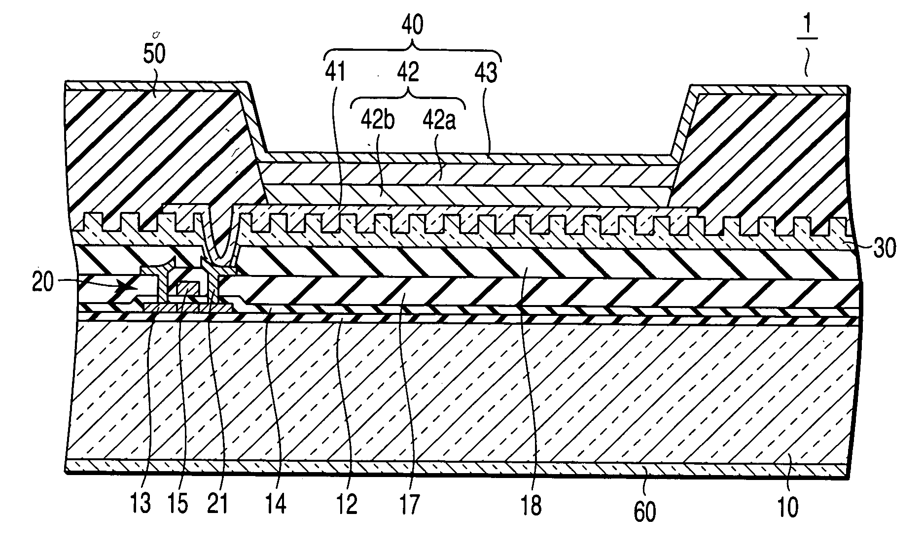
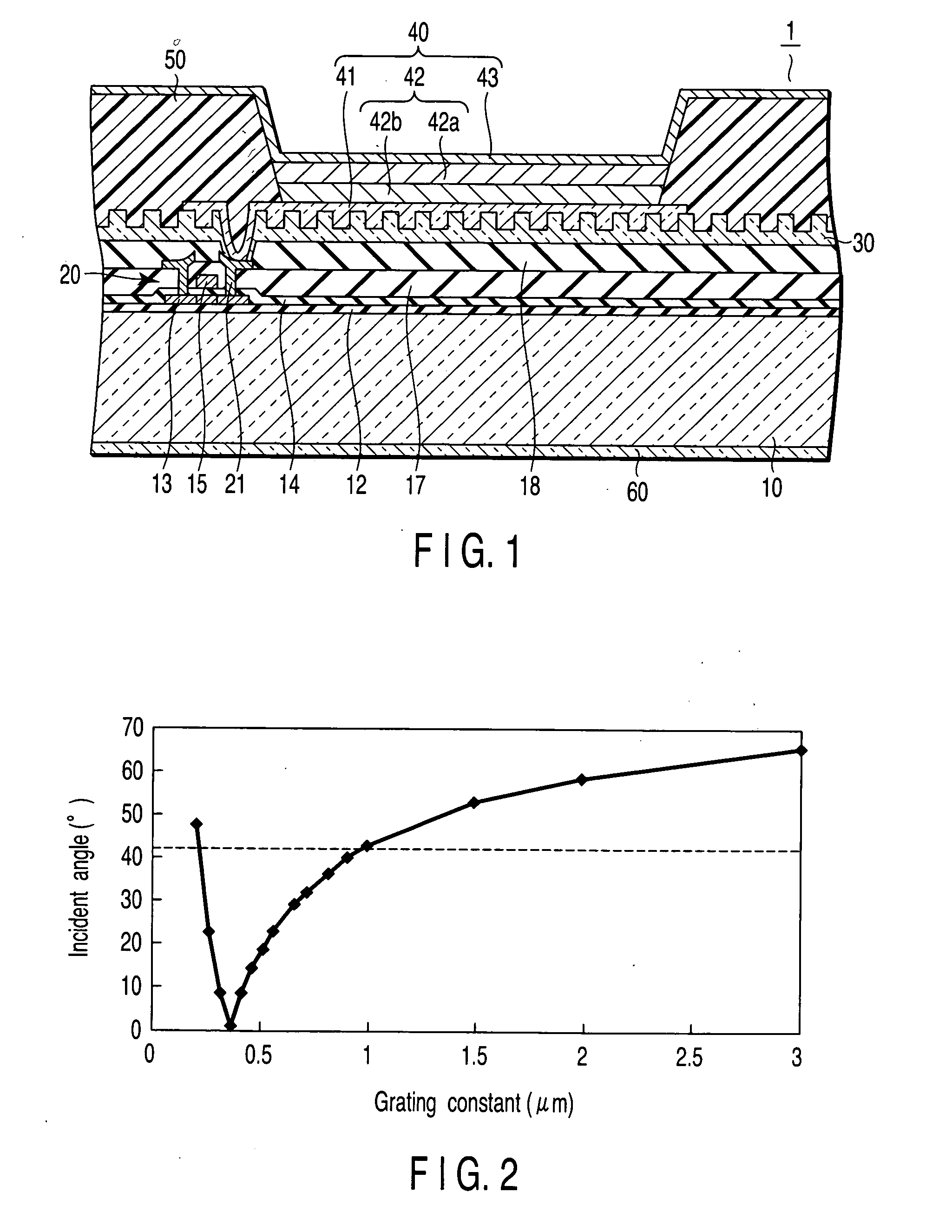
[0026]FIG. 1 is a partial sectional view schematically showing an optical device according to the present invention. FIG. 1 illustrates a self-emission display and, more specifically, an organic EL display 1 as an example of the optical device. Referring to FIG. 1, the display surface, i.e., the front surface of the organic EL display 1 is directed downward, and the back surface is directed upward.

[0027] The organic EL display 1 is a bottom emission type organic EL display which employs an active matrix drive method. The organic EL display 1 includes a transparent substrate 10 such as a glass substrate as an insulating layer with light transmission property.

[0028] On the transparent substrate 10, pixels are arranged in a matrix form. Each pixel includes, for example, an element control circuit (not shown), an output switch 20, an organic EL element 40, which are connected in series between a pair of power source terminals, and a pixel switch (not shown). The control terminal of the...

second embodiment

[0067] the present invention will be described next.

[0068]FIG. 8 is a sectional view schematically showing an organic EL display according to the second embodiment of the present invention. FIG. 8 illustrates an organic EL display 1 with its front surface directed upward and its back surface directed downward.

[0069] The organic EL display 1 is a top emission type organic EL display. Hence, unlike the first embodiment, a substrate 10 need not have a light transmitting property.

[0070] As in the first embodiment, an undercoat layer 12, TFT, interlayer insulating film 17, and passivation film 18 are sequentially formed on the substrate 10. Contact holes are formed in a gate insulator 14 and the interlayer insulating film 17 and passivation film 18. Source and drain electrodes 21 are electrically connected to the source and drain of the TFT via the contact holes.

[0071] A reflecting layer 70 and a first portion 31 (integrated with the passivation film 18) of a diffraction grating 30 ar...


PUM


Abstract

An optical device includes a first waveguide layer in which multiple-beam interference occurs, a second waveguide layer which includes a back surface facing the first waveguide layer and a front surface as a light output surface, and a diffraction grating which is arranged on a back side of the second waveguide layer and faces the first waveguide layer, wherein a grating constant of the diffraction grating is defined such that a first-order diffracted light emerges from the second waveguide layer, the first-order diffracted light being generated when a light component having a highest intensity of light which propagates in an in-plane direction while causing multiple reflection in the first waveguide layer enters the diffraction grating.

Description

CROSS-REFERENCE TO RELATED APPLICATIONS [0001] This is a Continuation Application of PCT Application No. PCT / JP2004 / 011615, filed Aug. 12, 2004, which was published under PCT Article 21(2) in Japanese. [0002] This application is based upon and claims the benefit of priority from prior Japanese Patent Application No. 2003-293111, filed Aug. 13, 2003, the entire contents of which are incorporated herein by reference. BACKGROUND OF THE INVENTION [0003] 1. Field of the Invention [0004] The present invention relates to an optical device such as an organic EL (electroluminescent) display. [0005] 2. Description of the Related Art [0006] Since organic EL displays are of self-emission type, they have a wide viewing angle and a high response speed. Further, they do not require a backlight, and therefore, low profile and light weight are possible. For these reasons, the organic EL displays are attracting attention as a display which replaces the liquid crystal display. [0007] An organic EL ele...

Claims


Application Information

Patent Timeline
IPC IPC(8): H01S3/03G09F9/30G02B5/18H01L27/32H01L51/50H01L51/52H05B33/00H05B33/02H05B33/12H05B33/14H05B33/24
CPCH01L27/3211H01L51/5275H01L51/5268H01L27/3244H10K59/35H10K59/12H10K50/854H10K50/858H05B33/22H05B33/02H05B33/12G02B5/18
Inventor OKUTANI, SATOSHIUEMURA, TSUYOSHIKUBOTA, HIROFUMIOKADA, NAOTADATONOTANI, JUNICHISUZUKI, KEIJIOOKAWA, HIDEKI
Owner JAPAN DISPLAY INC
Why Eureka
Try Eureka