

Optical module
a technology of optical modules and printed circuit boards, applied in the field of optical modules, can solve the problems of difficult to realize the positional accuracy of printed circuit boards, take a long period of time for a module assembly step, etc., and achieve the effects of reducing cross talk, facilitating the assembling step, and ensuring the positional accuracy of the printed circuit boards
- Summary
- Abstract
- Description
- Claims
- Application Information
AI Technical Summary
Benefits of technology
Problems solved by technology
Method used
Image

Examples
first modification
(A1) A First Modification
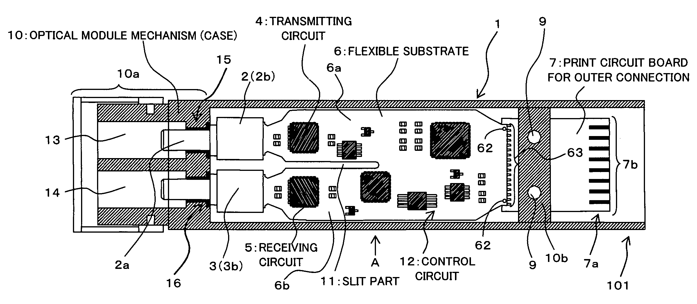
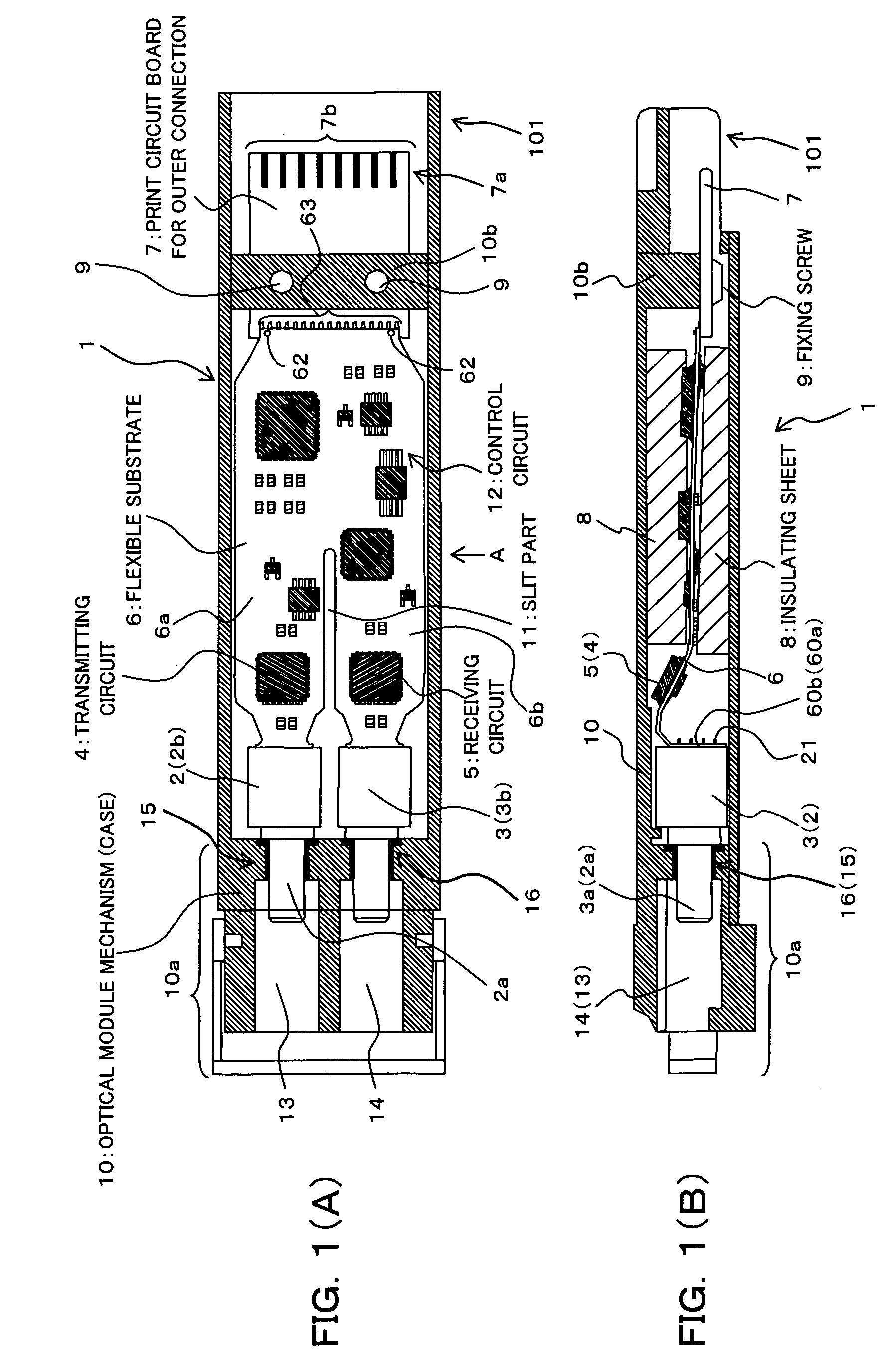
[0061]FIG. 4 (A) is a schematic plan view showing an inner structure of the XFP module 1 when employing the ceramic terminal package device described above with reference to FIG. 2(B) as the above-described respective optical devices 2, 3. FIG. 4(B) is an A arrow side view in FIG. 4 (A). In FIGS. 4(A) and 4(B), the elements provided with the same reference numerals as the above-described reference numerals are the same as the above-described elements or the similar to them except for a special case.
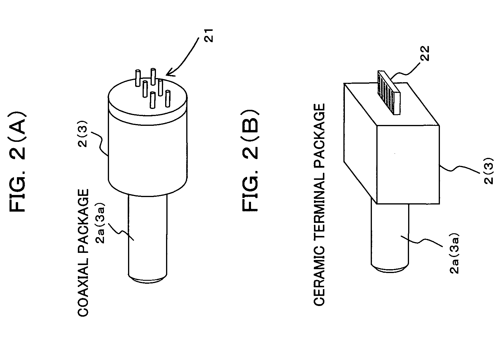
[0062] As shown in FIGS. 4(A) and 4(B), when employing the ceramic terminal package device as respective optical devices 2, 3, not the through hole electrode 61 described above with reference to FIG. 3(A) but a connection electrode 64 same as the connection electrode 63 at the substrate 60c of the flexible substrate 6 is provided as end portions 60a and 60b of respective branch portions 6a and 6b of the flexible substrate 6, respectively, so that the connection e...
second modification
(A2) A Second Modification
[0064] In addition, according to the above-described embodiment and the first modification, all electronic circuit device groups including the transmitting circuit 4, the receiving circuit 5, and the control circuit group 12 are mounted on the flexible substrate 6, however, if the positional accuracy between the case 10 and the print circuit board6 (the common difference of the outline of the print circuit board) can be secured, for example, as shown in FIG. 5, appropriately changing the size of the print circuit board 7 appropriately, a portion of these electronic circuit device group (in the embodiment of FIG. 5, a portion of the control circuit group 12) may be mounted on the print circuit board 7.
[0065] For example, the part suitable to be mounted on the print circuit board 7 rather than the flexible substrate 6 [the part or the like that BGA (a soldering ball is mounted) is preferable] is preferably mounted on the print circuit board 7, and the electr...
third modification
(A3) A Third Modification
[0067]FIG. 6 is a schematic plan view showing a third modification of the above-described XFP module. The XFP module 1 shown in this FIG. 6 is largely different from the above-described one in that the optical transmitting device 2 and the print circuit board 7 are electrically connected by the independent flexible substrate 6-1, and the optical receiving device 3 and the print circuit board 7 are electrically connected by the independent flexible substrate 6-2, respectively. In other words, this is equivalent to that the slit part 11 is elongated to the print circuit board 7 and the flexible substrate 6 is divided into two, namely, the flexible substrates 6-1 and 6-2. Then, mounting the transmitting circuit 4 on the flexible substrate 6-1 to be connected to an optical transmission module 2, a receiving circuit 5 is mounted on the flexible substrate 6-2 to be connected to an optical transmission module 3.
[0068] Thus, by dividing the substrates mounted on th...
PUM
 Abstract
Description
Claims
Application Information