Semiconductor device and manufacturing method thereof

a semiconductor and semiconductor technology, applied in semiconductor/solid-state device manufacturing, basic electric elements, electric devices, etc., can solve the problems of reducing the idsat the nitride layer cannot be formed by such thermal nitridation, and the charge mobility may be decreased due to a decrease in the charge mobility, so as to prevent boron penetration and minimize the effect of the charge mobility decrease in the nmos devi

Inactive Publication Date: 2006-03-23
DONGBU ELECTRONICS CO LTD
View PDF5 Cites 5 Cited by
  • Summary
  • Abstract
  • Description
  • Claims
  • Application Information

AI Technical Summary

Benefits of technology

[0011] The present invention has been made in an effort to provide a semiconductor device and a manufacturing method thereof having advantages of preventing boron penetration in a PMOS device and minimizing a decrease of charge mobility in an NMOS device.

Problems solved by technology

However, although the oxynitride layer has many merits for a PMOS transistor, it has a drawback for an NMOS transistor in that a saturation current (Idsat) may be decreased due to a decrease of charge mobility.
Such a drawback may be caused because nitrogen can be deposited at the interface between the silicon substrate and the oxide layer, thereby decreasing the charge mobility.
However, for a semiconductor device of less than a 90 nm line scale, the nitride layer cannot be formed by such thermal nitridation, since such a thermal nitride layer does not provide desired transistor performance.

Method used


Image

  • Semiconductor device and manufacturing method thereof
  • Semiconductor device and manufacturing method thereof
  • Semiconductor device and manufacturing method thereof

Examples


Embodiment Construction

[0027] An exemplary embodiment of the present invention will hereinafter be described in detail with reference to the accompanying drawings.

[0028] With reference to the accompanying drawings, the present invention will be described in order for those skilled in the art to be able to implement the invention. As those skilled in the art would realize, the described embodiments may be modified in various different ways, all without departing from the spirit or scope of the present invention.

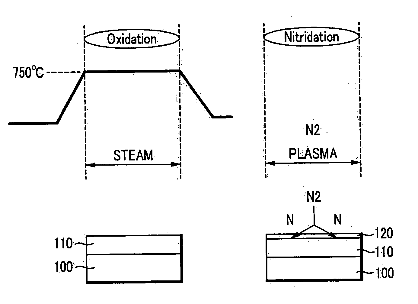
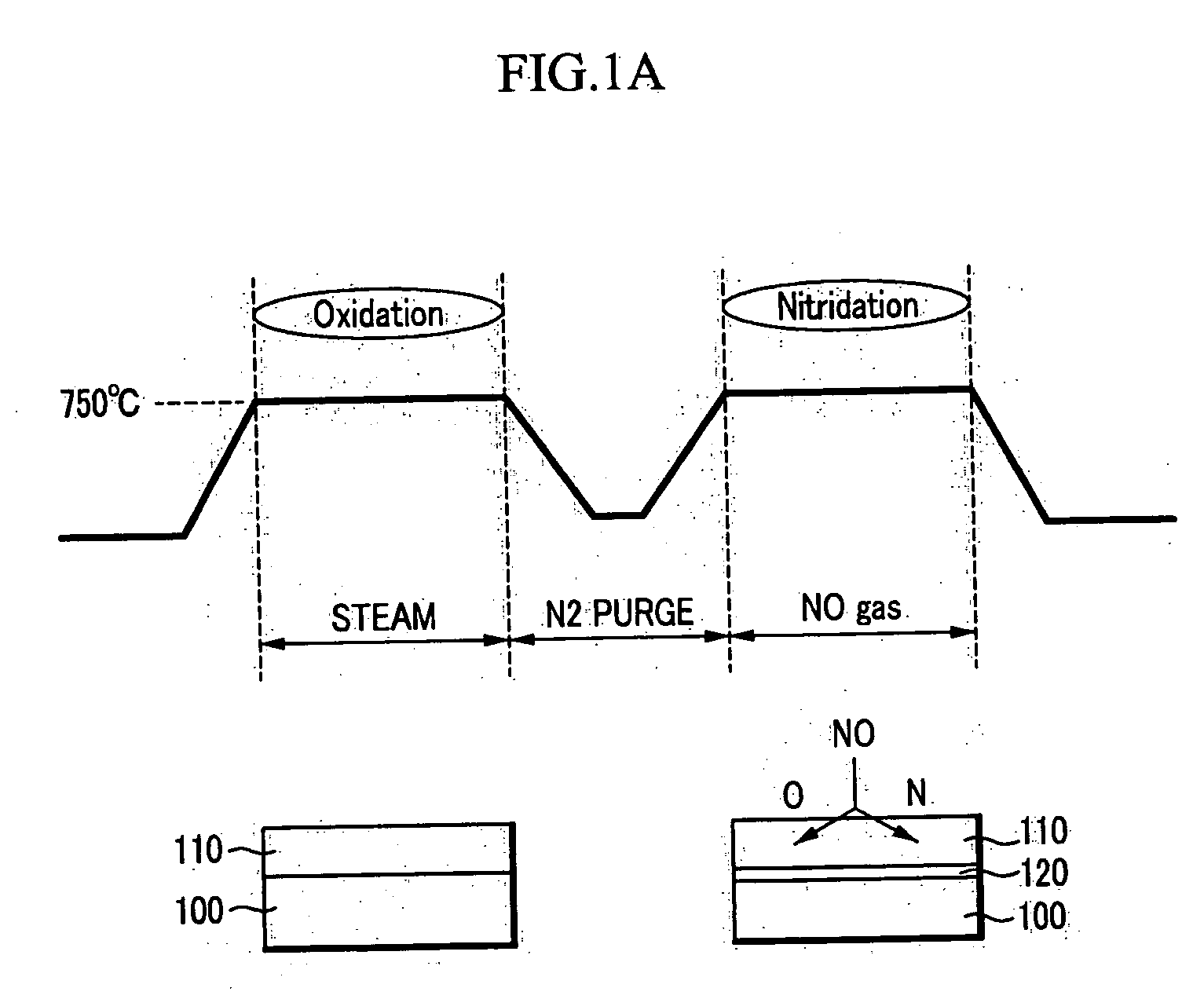
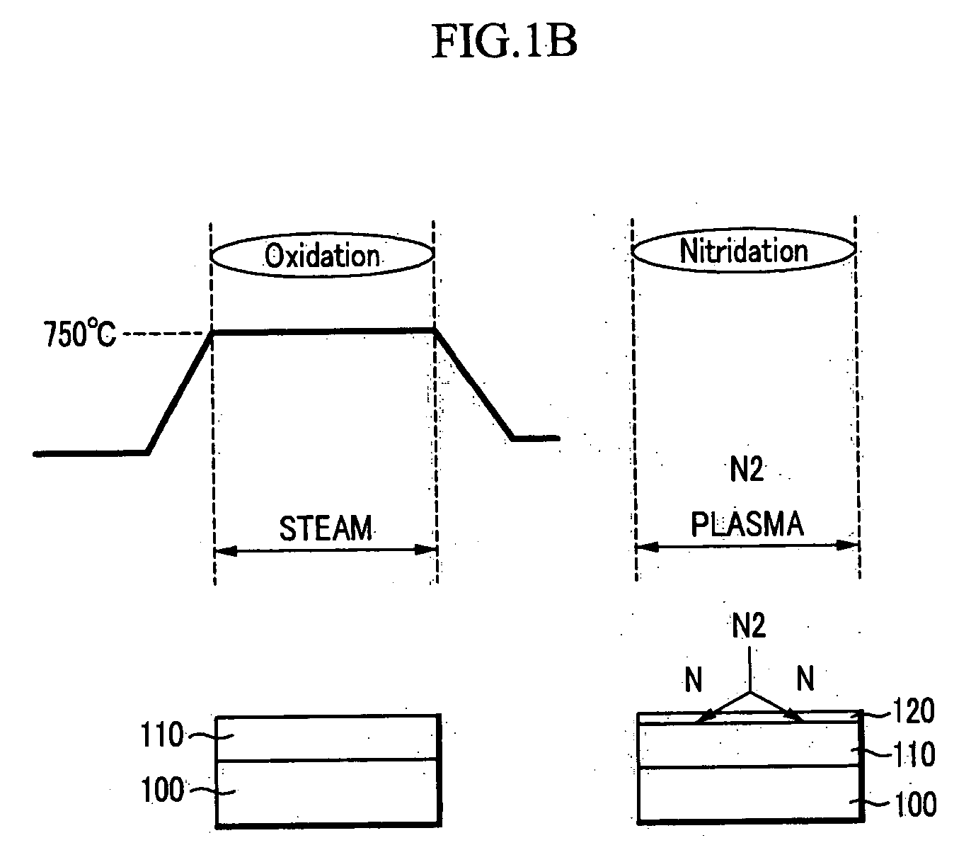
[0029]FIG. 1A illustrates a method for thermally a nitride layer, and FIG. 1B illustrates a method for forming a nitride layer using plasma. Nitridation methods may be classified into thermal nitridation methods and plasma nitridation methods.

[0030] In addition, gate oxide formation methods may be classified into torch methods and water vapor generator (WVG) methods, depending on how water or steam (H2O) is generated. The WVG method may form a thinner oxide layer. The water or steam is typically ...


PUM


Abstract

A method of manufacturing a semiconductor device includes forming a gate oxide layer on a substrate and forming a nitride layer on the surface of the oxide layer using nitrogen at a concentration of 9 to 11% as a plasma gas. With such scheme, the plasma nitridation method is used so that charge mobility can be preserved for an NMOS transistor and the boron penetration is prevented for a PMOS transistor in a semiconductor having a gate length of 100 nm or less.

Description

CROSS-REFERENCE TO RELATED APPLICATION [0001] This application claims priority to and the benefit of Korean Patent Application No. 10-2004-0074497 filed in the Korean Intellectual Property Office on Sep. 17, 2004, the entire contents of which are incorporated herein by reference. BACKGROUND OF THE INVENTION [0002] (a) Field of the Invention [0003] The present invention relates to a semiconductor device and a manufacturing method thereof. [0004] (b) Description of the Related Art [0005] Generally, a gate-insulating layer has involved a silicon oxide layer in a MOSFET. As semiconductor devices are becoming more highly integrated and an operation speed thereof is increasing, a gate-insulating layer therein is becoming thinner and thinner. Accordingly, because of the thinness of the gate-insulating layer, boron penetration may sometimes occur between a gate electrode and a silicon substrate. Accordingly, for a semiconductor device having a very fine line structure (e.g., less than 0.18 ...

Claims


Application Information

Patent Timeline
Patent Type & Authority Applications(United States)
IPC IPC(8): H01L21/336
CPCH01L21/28202H01L21/18
Inventor KIM, JEA-HEE
Owner DONGBU ELECTRONICS CO LTD
Why Eureka
Try Eureka