Singulation method used in image sensor packaging process and support for use therein

Active Publication Date: 2006-03-23
ADVANCED SEMICON ENG INC
View PDF9 Cites 1 Cited by
  • Summary
  • Abstract
  • Description
  • Claims
  • Application Information

AI Technical Summary

Benefits of technology

[0009] To achieve the above listed and other objects, a singulation method having features of the present invention is accomplished by a sawing operation instead of the punching operation mentioned above such that the substrate for use with the present invention can be designed to have units arranged at high density thereby significantly decreasing the manufacturing cost. In the singulation method of the present invention, the semi-finished product is placed on a support having a plurality of cavities such that the package structures are respectively received in the cavities of the support. Then, the semi-finished product is sawed into separate image sensor packages. During the sawing step, the package structures are positioned precisely and clamped in place with the support whereby the dimension change of finished image sensor packages can be controlled within a desired range, e.g., ±0.1 mm. Specifically, the package structures may be positioned precisely and clamped in place by a suction within the cavities created by decreasing the air pressure in the cavities. Alternatively, the suction may be created by decreasing the air pressure in a plurality of first slots provided between the cavities of the support. Note that the support for use with the present invention is configured to have a gap between the transparent component and the support when the support abuts against at least a portion of the housing of each package structure during the sawing step. Such kind of support design can protect the transparent component from damage of the support when the package structures are clamped by the support.
[0010] Note that the development and manufacture of a support for use with the present invention usually takes much less time than the development and manufacture of a punching tool. Therefore, assembly lead time can be significantly shortened by using the singulation method of the present invention.

Problems solved by technology

However, such a punching operation requires a substrate having a low-density unit designs which significantly increases the manufacturing cost because the substrate accounts for up to 60% of the total assembly cost.
In addition, the biggest drawback of such a punching operation is that every different shape or size of packages requires a dedicated punching tool, e.g., if the shape or the size is altered, the punching tool must be redesigned.
The development and manufacture of a punching tool typically takes about 3˜4 months thereby significantly increasing assembly lead time.
This is unacceptable since current image sensor packages have very short lifetimes (typically about 3˜6 months).

Method used


Image

  • Singulation method used in image sensor packaging process and support for use therein
  • Singulation method used in image sensor packaging process and support for use therein
  • Singulation method used in image sensor packaging process and support for use therein

Examples


Embodiment Construction

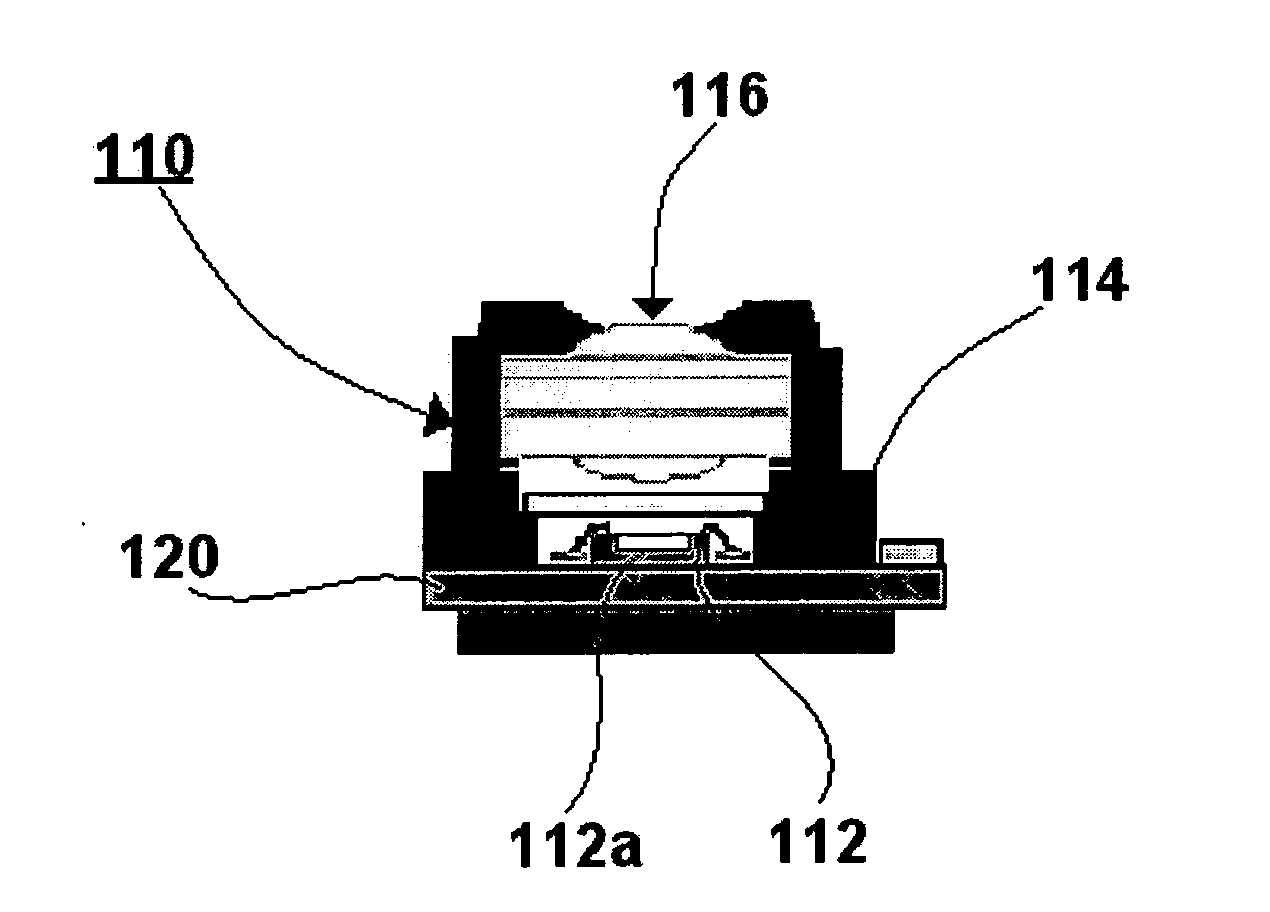
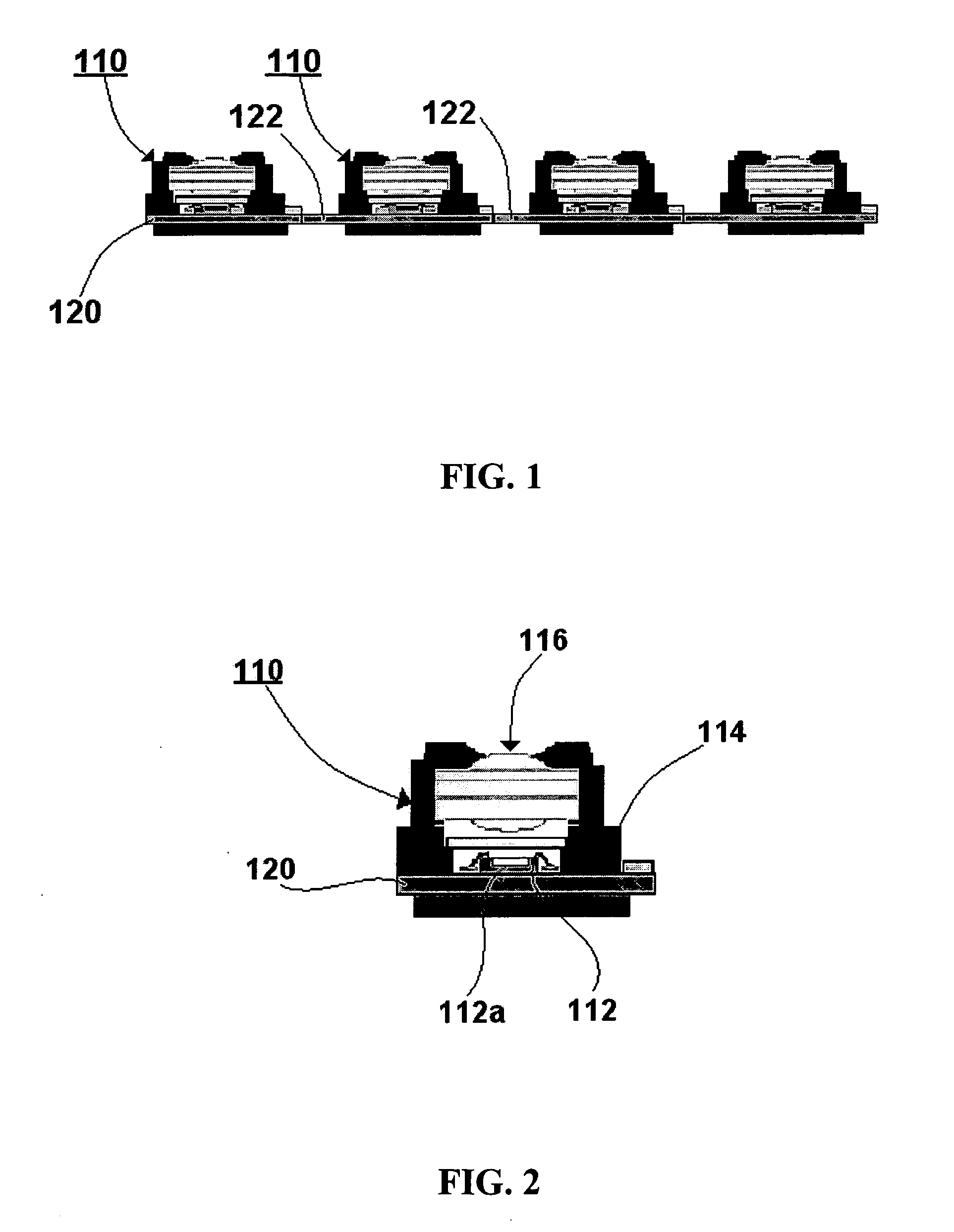
[0017] The present invention is directed to a singulation method used in a process for making a plurality of image sensor packages. In the image sensor packaging process for use with the present invention, a semi-finished product (see FIG. 1) is formed by packaging a plurality of image sensor chips 112 (see FIG. 2) into an array of package structures 110 on a substrate 120, e.g., a liquid crystal polymer (LCP) substrate, a thermoplastic substrate, an alumina-based ceramic substrate, a printed circuit board, a plastic glass laminated substrate, or a tape-based substrate.

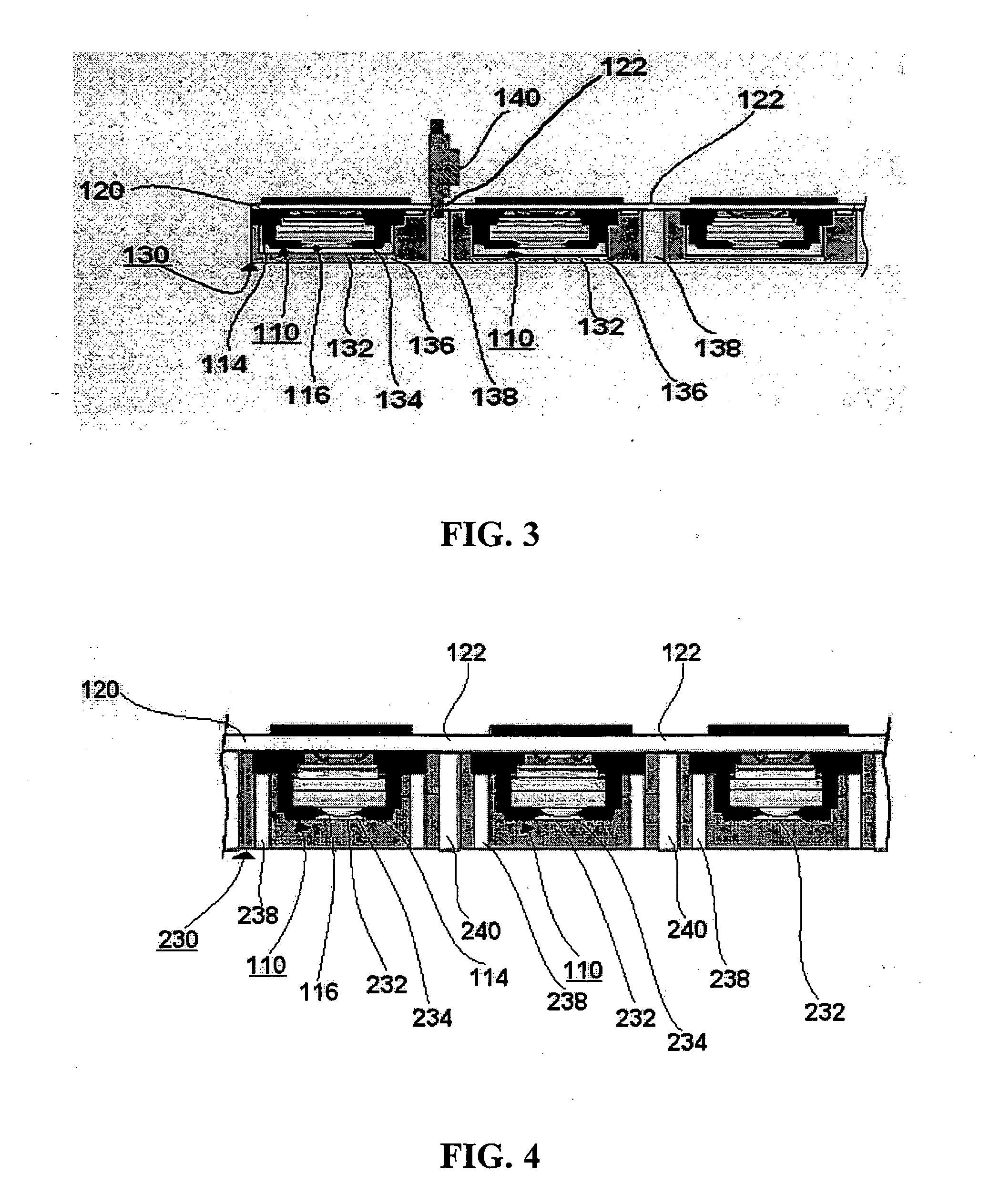
[0018] As shown in FIG. 1, the package structures 110 are arranged in strip type configuration and separated from each other by a plurality of cutting streets 122. However, the package structures 110 may be arranged in rows and columns, e.g., a 4×4 matrix or a 4×8 matrix, which is more appropriate for mass production. When an matrix type arrangement is adopted, the cutting streets generally form an orthogonal grid on...


PUM


Abstract

A singulation method used in a process for making a plurality of image sensor packages is disclosed. Firstly, a semi-finished product including a plurality of package structures formed on a substrate is placed on a support having a plurality of cavities for receiving the package structures. Then, the semi-finished product is sawed into separate image sensor packages. During the sawing step, the air pressure in the cavities is decreased to create suction within the cavities such that the support abuts against at least a portion of the housing of each package structure with a gap between the transparent component and the support whereby the package structures are positioned precisely and clamped in place with the support during the sawing step.

Description

BACKGROUND OF THE INVENTION [0001] 1. Field of the Invention [0002] This invention relates to a process for making image sensor packages and more specifically to a singulation method used in the image sensor packaging process. [0003] 2. Description of the Related Art [0004] Image sensors are increasingly in demand for incorporation into electronic devices. They may be used for a variety of applications including consumer electronics like digital cameras, cellular telephones and hand-held scanners. [0005] In order to protect the image sensors in the form of an integrated circuit die, i.e., the image sensor chip, from physical damage and from contaminants in the surrounding environment, it is the practice to place the image sensor chip in a package. The package typically includes an opening sealed by a transparent lid to allow light or other forms of electromagnetic radiation to pass through to sensing circuitry on the active surface of the image sensor chip. Another purpose of the pa...

Claims


Application Information

Patent Timeline
IPC IPC(8): H01L21/78H01L21/50
CPCH01L27/14625H01L27/14618H01L2224/45144H01L2224/48091H01L2924/00014H01L2924/00
Inventor YANG, JUN YOUNGKIM, IN HO
Owner ADVANCED SEMICON ENG INC
Why Eureka
Try Eureka