Photovoltaic device
a photovoltaic and solar cell technology, applied in the field of photovoltaic devices, can solve the problems of deteriorating and achieve the effect of reducing the activation rate of boron (a, decreasing the built-in electric field, and deteriorating the output characteristics of solar cells
- Summary
- Abstract
- Description
- Claims
- Application Information
AI Technical Summary
Benefits of technology
Problems solved by technology
Method used
Image

Examples
first embodiment
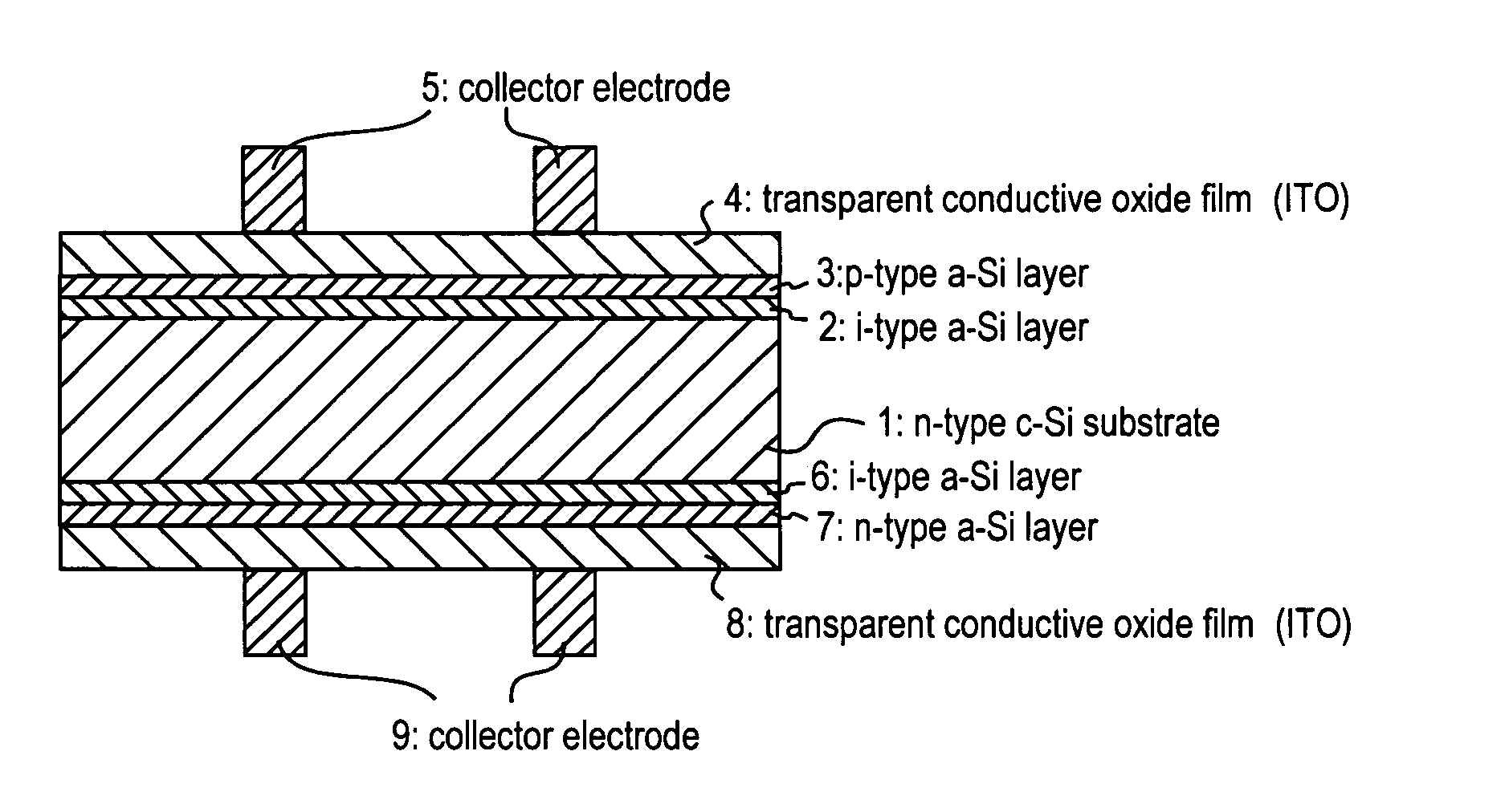
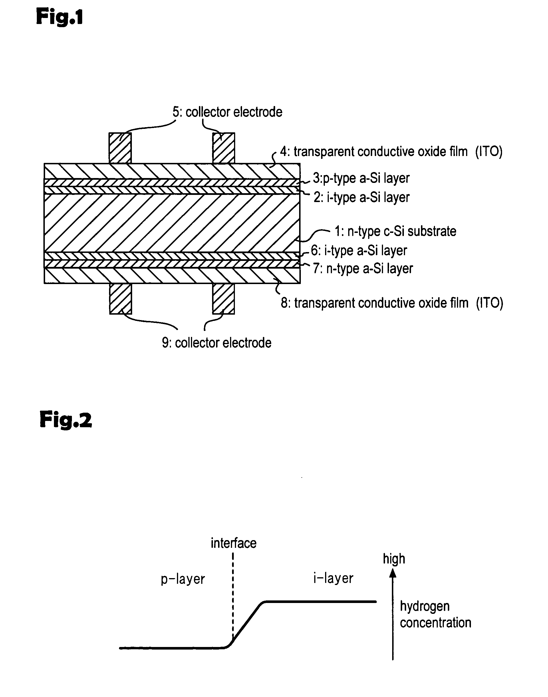
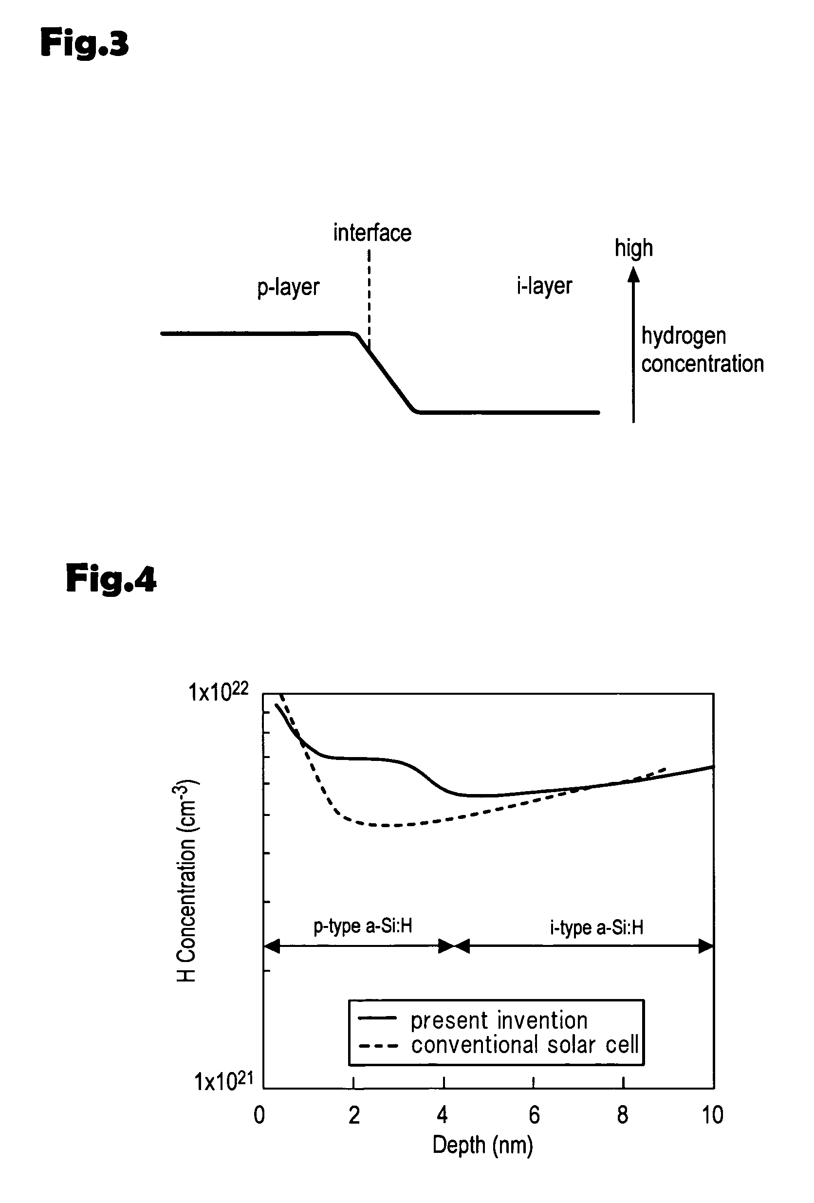
[0066] A solar cell was prepared with the p-type amorphous silicon layer 3 formed with more hydrogen dilution than that for the i-type amorphous silicon layer. Table 2 shows specific conditions to form the p-type amorphous silicon layer 3 and the i-type amorphous silicon layer 2 on the front surface of the substrate. Layers on the rear surface of the substrate are formed under conditions shown in Table 1. In addition, the i-type amorphous silicon layer 2 and the p-type amorphous silicon layer 3 were formed so as to have thicknesses of 10 nm and 5 nm, respectively.
TABLE 2conditionsSubstratetemperaturepower(degreespressuredensityprocesscentigrade)gas(Pa)(mW / cm2)fronthydro-170H2: 100 sccm5015genationi-type a-Si170H2: 100 sccm5015SiH4: 40 sccmp-type a-Si170H2: 400 sccm5015SiH4: 40 sccm2% B2H6 / H2:20 sccm
[0067] In compliance with Table 2, the p-type amorphous silicon layer 3 was formed with more hydrogen dilution than that used to form the i-type amorphous silicon layer in order to form ...
second embodiment
[0074] Table 3 shows formation conditions of the As appreciated from Table 3, the p-type amorphous silicon layer 31 and the p-type amorphous silicon layer 32 were formed with different flow rates of B2H6. More amount of B2H6 flow was used for the p-type amorphous silicon layer 32 than that for the p-type amorphous silicon layer 31, while more amount of the hydrogen dilution was used for the p-type amorphous silicon layer 31. Layers on the rear surface of the substrate were formed under the conditions shown in Table 1. The i-type amorphous silicon layer 2 was formed to have a thickness of 10 nm, while the p-type amorphous silicon layers 31 and 32 have a thickness of 4 nm each.
TABLE 3conditionsSubstratetemperaturePower(degreespressureDensityprocesscentigrade)gas(Pa)(mW / cm2)fronthydro-170H2: 100 sccm5015genationi-type a-Si170H2: 100 sccm5015SiH4: 40 sccmp-type a-Si170H2: 400 sccm5015(31)SiH4: 20 sccmB2H6: 10 sccmp-type a-Si170H2: 100 sccm5015(32)SiH4: 40 sccm2% B2H6 / H2:40 sccm
[0075] A...
third embodiment
[0079] The formation conditions of the third embodiment are shown in Table 4. Layers on the rear surface of the substrate were formed under the conditions shown in Table 1. The thickness of the i-type amorphous silicon layer 2 including the i-type trap layer 33 is 10 nm, (i-type trap layer 33 has a thickness of 2 nm alone). The p-type amorphous silicon layer 3 has a thickness of 8 nm.
TABLE 4conditionsSubstratetemperaturePower(degreespressuredensityprocesscentigrade)gas(Pa)(mW / cm2)fronthydro-170H2: 100 sccm5015genationi-type a-Si170H2: 100 sccm5015SiH4: 40 sccmi-type a-Si170SiH4: 40 sccm5015traplayer (33)p-type a-Si170H2: 100 sccm5015SiH4: 40 sccm2% B2H6 / H2:40 sccm
[0080] In the third embodiment, no hydrogen dilution was used to form the i-type trap layer 33 in order to make the hydrogen concentration in the i-type trap layer 33 lower than that in the i-type amorphous silicon layer. There are some other ways as indicated below.
[0081] (1) The temperature of the substrate during the fo...
PUM
| Property | Measurement | Unit |
|---|---|---|
| Thickness | aaaaa | aaaaa |
| Thickness | aaaaa | aaaaa |
| Thickness | aaaaa | aaaaa |
Abstract
Description
Claims
Application Information
 - R&D
- Intellectual Property
- Life Sciences
- Materials
- Tech Scout
- Unparalleled Data Quality
- Higher Quality Content
- 60% Fewer Hallucinations
Browse by: Latest US Patents, China's latest patents, Technical Efficacy Thesaurus, Application Domain, Technology Topic, Popular Technical Reports.
© 2025 PatSnap. All rights reserved.Legal|Privacy policy|Modern Slavery Act Transparency Statement|Sitemap|About US| Contact US: help@patsnap.com