Finfet sram cell using inverted finfet thin film transistors

a thin film transistor and inverted finfet technology, applied in the field of integrated circuits, can solve the problems of unabated demand for higher and higher density srams, and achieve the effects of reducing surface area, reducing the number of transistors, and simplifying the layou

Inactive Publication Date: 2006-03-30
TAIWAN SEMICON MFG CO LTD
View PDF8 Cites 63 Cited by
  • Summary
  • Abstract
  • Description
  • Claims
  • Application Information

AI Technical Summary

Benefits of technology

[0003] The present invention provides an inverted FinFET thin film transistor, and a static random access memory (SRAM) cell that is formed using inverted F...

Problems solved by technology

Although many techniques have been successfully employed to provide higher ...

Method used


Image

  • Finfet sram cell using inverted finfet thin film transistors
  • Finfet sram cell using inverted finfet thin film transistors
  • Finfet sram cell using inverted finfet thin film transistors

Examples


Embodiment Construction

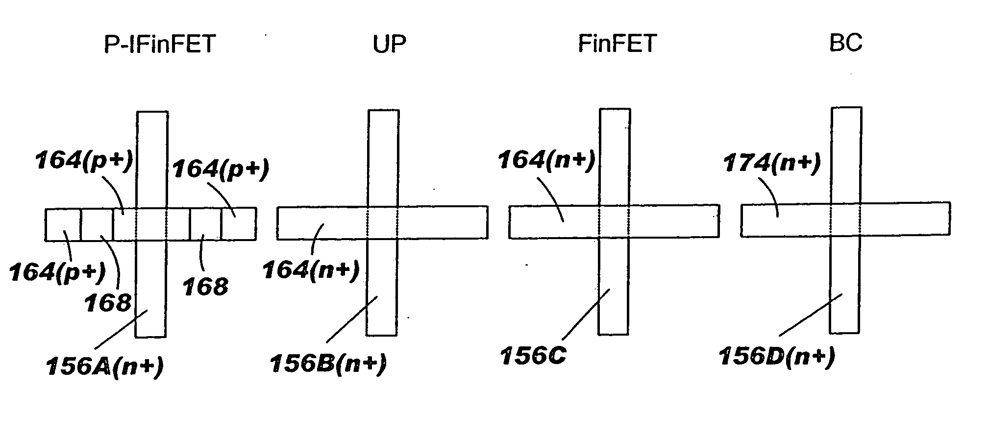
[0023] The present invention addresses the above-mentioned problems, as well as others, by providing an inverted FinFET thin film transistor, and a static random access memory (SRAM) cell that is formed using inverted FinFET thin film transistors.

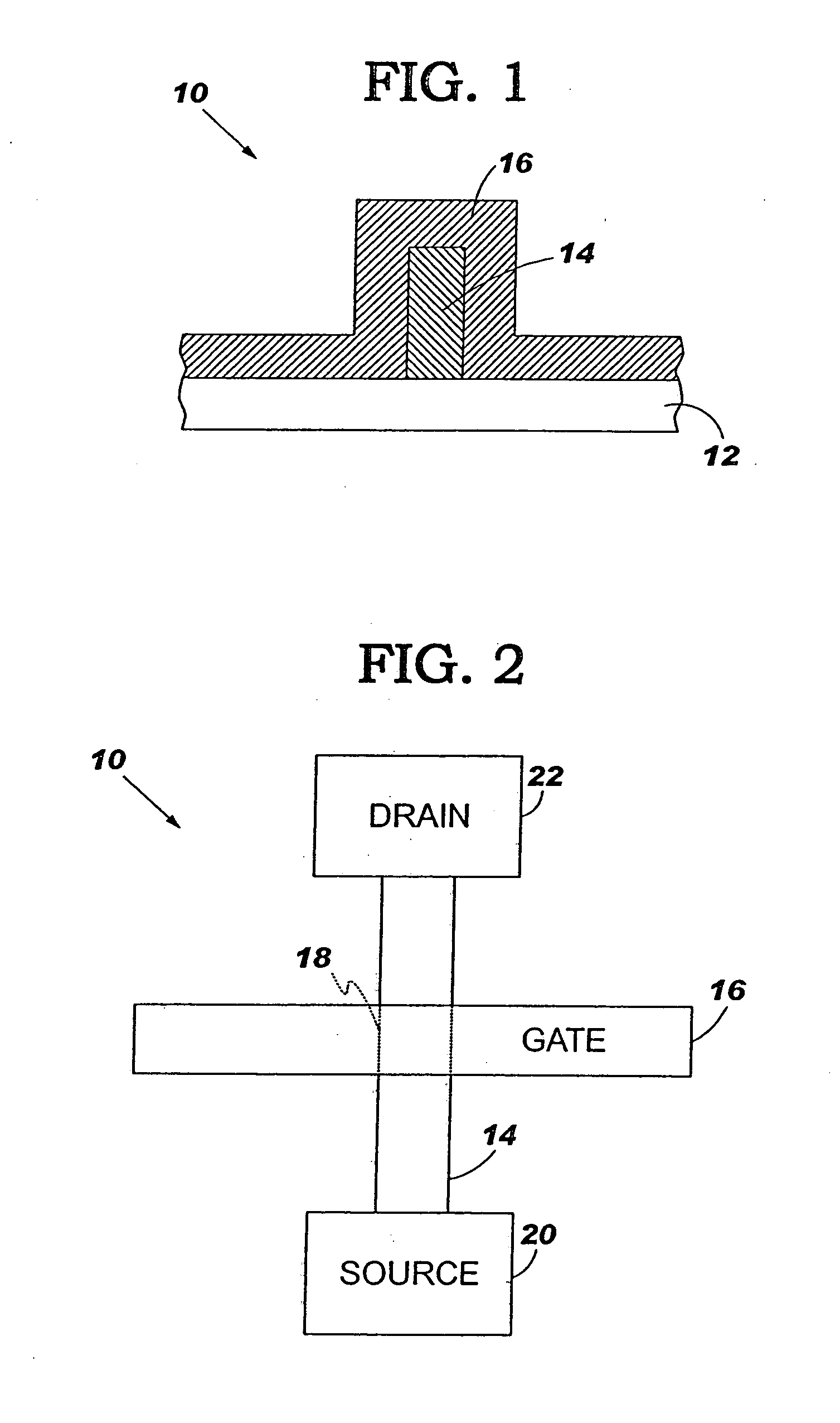
[0024] A cross-sectional view of a conventional FinFET thin film transistor 10 is illustrated in FIG. 1. A plan view of the FinFET transistor 10 is illustrated in FIG. 2. In this example, the FinFET transistor 10 is formed on an insulating layer 12 (e.g., a layer of SiO2). The FinFET transistor 10 comprises a fin 14, typically formed of silicon or other suitable semiconductor material, and a gate 16, formed of polysilicon or other suitable conductive material, running over the fin 14. A channel 18 is formed in the portion of the fin 14 that extends under the gate 16. As shown in FIG. 2, the source 20 and drain 22 of the FinFET transistor 10 are located at opposing ends of the fin 14. The benefits provided by such a FinFET transistor 10 inc...


PUM


Abstract

An integrated circuit, such as a SRAM cell (130), including an inverted FinFET transistor (P2) and a FinFET transistor (N3). The inverted FinFET transistor includes a first gate region (108) formed by semiconductor structure (100) on a substrate, a first body region comprised of a semiconductor layer (104), having a first channel region (112) disposed on the first gate region and a source (110) and drain (114) formed on either side of the first channel region. The FinFET transistor (N3) is coupled to the inverted FinFET transistor, and includes a second body region formed by the semiconductor structure (102), having a second channel region (118), and a source (116) and drain (120) formed on either side of the second channel region, and a second gate region (122) comprised of the semiconductor layer, disposed on the second channel region.

Description

TECHNICAL FIELD [0001] The present invention relates in general to integrated circuits. More particularly, the present invention is directed to an inverted FinFET thin film transistor, and a static random access memory (SRAM) cell that is formed using inverted FinFET thin film transistors. BACKGROUND ART [0002] One important characteristic of a SRAM cell is the surface area required to form the cell on an integrated circuit chip. By reducing the size of the SRAM cell, a higher density SRAM can be fabricated. Although many techniques have been successfully employed to provide higher density SRAMs, the demand for higher and higher density SRAMs continues unabated. Accordingly, there is a continuous need to produce ever smaller SRAM cells. DISCLOSURE OF THE INVENTION [0003] The present invention provides an inverted FinFET thin film transistor, and a static random access memory (SRAM) cell that is formed using inverted FinFET thin film transistors. The SRAM cell has a simplified layout...

Claims


Application Information

Patent Timeline
IPC IPC(8): H01L21/84H01L21/00H01L21/8238
CPCH01L21/84H01L27/11H01L29/785H01L27/1203H01L29/66787H01L27/1104H10B10/00H10B10/12
Inventor BREITWISCH, MATTHEWNOWAK, EDWARDJ
Owner TAIWAN SEMICON MFG CO LTD
Why Eureka
Try Eureka