Nonplanar transistors with metal gate electrodes

a metal gate electrode and transistor technology, applied in the direction of transistors, semiconductor devices, electrical equipment, etc., can solve the problems of increasing impracticality, decreasing the thickness of silicon films, and reducing the production efficiency of thin silicon films with thicknesses less than 10 nanometers, and achieving the effect of reducing the cost of manufacturing

Active Publication Date: 2006-04-06
TAHOE RES LTD
View PDF35 Cites 206 Cited by
  • Summary
  • Abstract
  • Description
  • Claims
  • Application Information

AI Technical Summary

Problems solved by technology

However, as gate lengths scale especially as they approach 30 nm, the need for ever decreasing silicon film thickness (TSi) makes this approach increasingly impractical.
The fabrication of thin silicon films with thicknesses of less than 10 nanometers, is considered to be extremely difficult.
On one hand, obtaining wafer uniformity on the order of one nanometer is a difficult challenge.
On the other hand, to be able to contact these thin films to form raised source/drain regions to decrease junction resistance, becomes almost impossible since the thin silicon layer in the source/drain regions becomes consumed during the gate etch and various cleans following the gate etc

Method used


Image

  • Nonplanar transistors with metal gate electrodes
  • Nonplanar transistors with metal gate electrodes
  • Nonplanar transistors with metal gate electrodes

Examples


Embodiment Construction

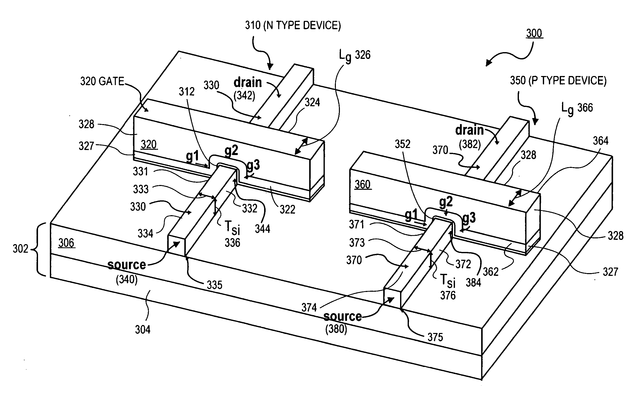
[0015] A nonplanar transistor having a gate electrode comprising a lower metal layer is described. In the following description numerous specific details are set forth in order to provide a thorough understanding of the present invention. In other instances, well known semiconductor processing techniques and features have not been described in particular detail in order to not unnecessarily obscure the present invention.

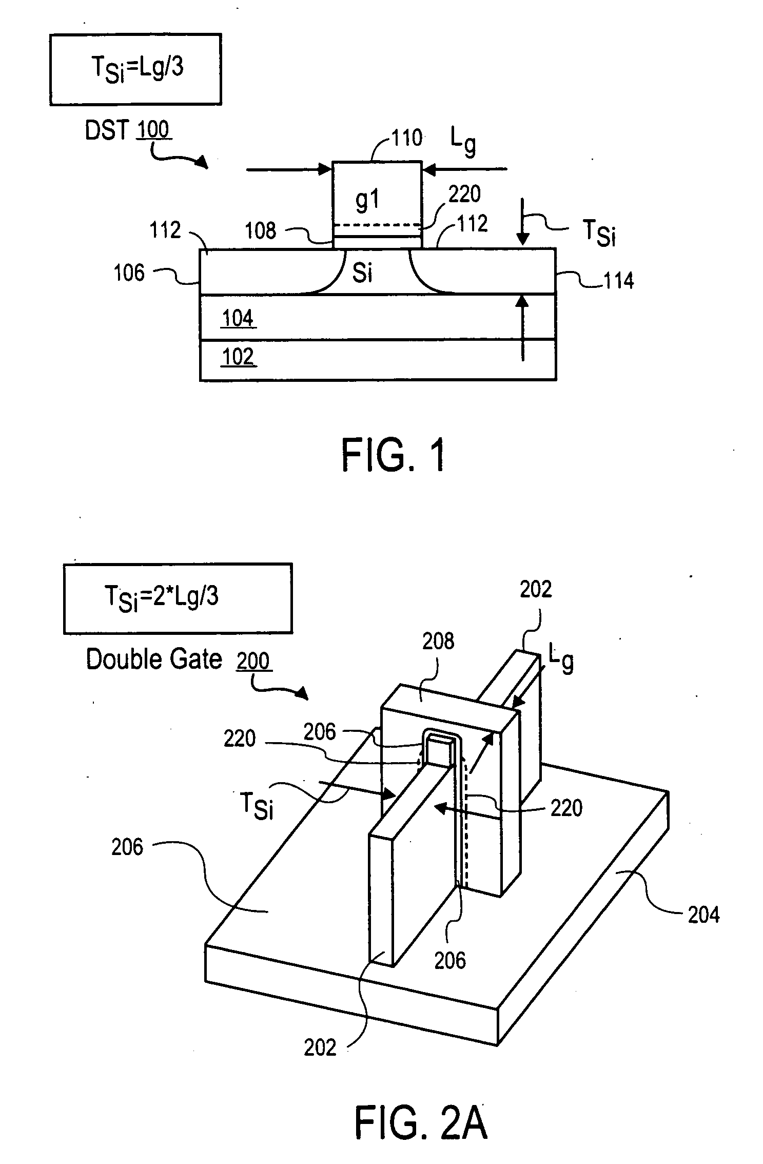
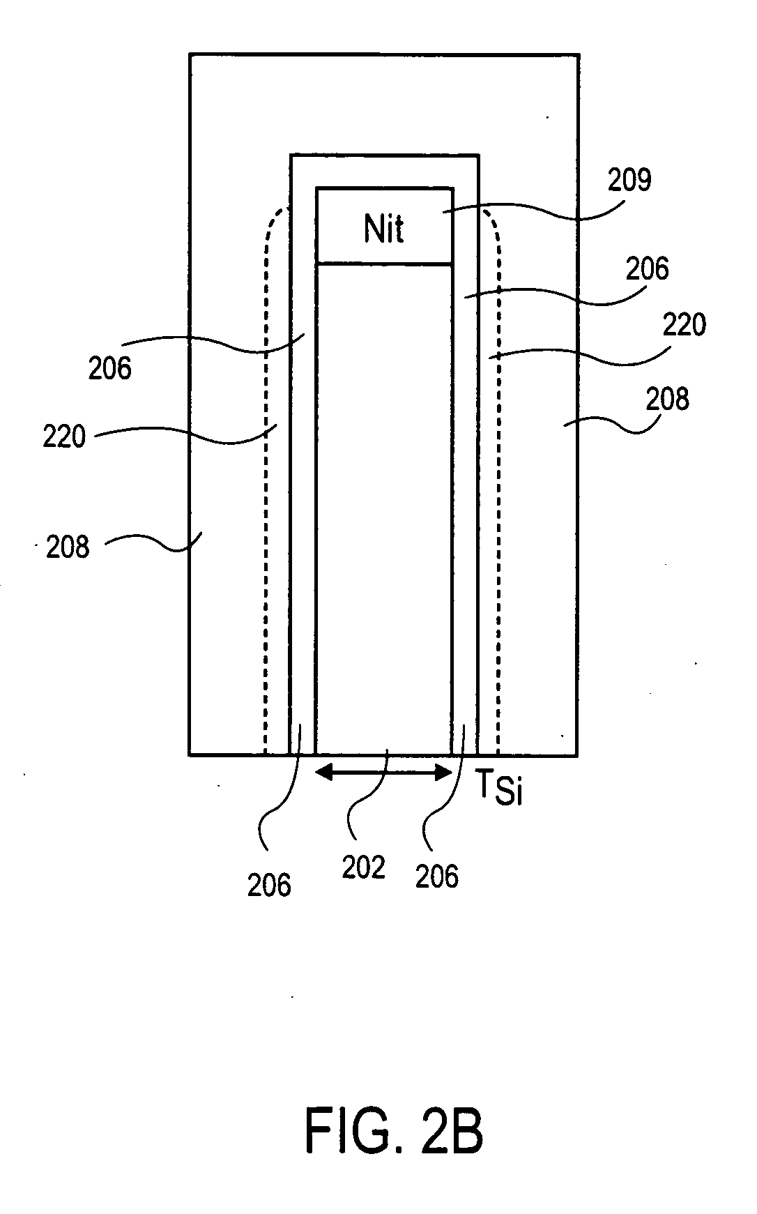
[0016] The present invention is a novel nonplanar transistor having a metal gate electrode and its method of fabrication. A nonplanar device includes a semiconductor body having a top surface and laterally opposite sidewalls formed on a substrate. A gate dielectric is formed on the top surface and on the sidewalls of the channel region of the semiconductor body. A metal gate electrode is then formed around the semiconductor body so that it covers the top surface and two sides of the semiconductor body. Since the gate electrode covers the semiconductor body on three ...


PUM


Abstract

A semiconductor device comprising a semiconductor body having a top surface and a first and second laterally opposite sidewalls as formed on an insulating substrate is claimed. A gate dielectric is formed on the top surface of the semiconductor body and on the first and second laterally opposite sidewalls of the semiconductor body. A gate electrode is then formed on the gate dielectric on the top surface of the semiconductor body and adjacent to the gate dielectric on the first and second laterally opposite sidewalls of the semiconductor body. The gate electrode comprises a metal film formed directly adjacent to the gate dielectric layer. A pair of source and drain regions are then formed in the semiconductor body on opposite sides of the gate electrode.

Description

BACKGROUND OF THE INVENTION [0001] 1. FIELD OF THE INVENTION [0002] The present invention relates to the field of semiconductor integrated circuit manufacturing, and more particularly to CMOS integrated circuits with p type and n type nonplanar transistors with metal gate electrodes and methods of fabrication. [0003] 2. DISCUSSION OF RELATED ART [0004] In order to increase device performance, silicon on insulator (SOI) transistors have been proposed for the fabrication of modern integrated circuits. FIG. 1 illustrates a standard fully depleted silicon on insulator (SOI) transistor 100. SOI transistor 100 includes a single crystalline silicon substrate 102 having an insulating layer 104, such as a buried oxide formed thereon. A single crystalline silicon body 106 is formed on the insulating layer 104. A gate dielectric layer 108 is formed on the single crystalline silicon body 106 and a gate electrode 110 formed on the gate dielectric 108. Source 112 and drain 114 regions are formed ...

Claims


Application Information

Patent Timeline
IPC IPC(8): H01L27/12
CPCH01L21/845H01L27/1211H01L29/66545H01L29/66795H01L29/785H01L29/66439H01L29/0673Y10S438/926Y10S438/974H01L29/41791
Inventor BRASK, JUSTIN K.DOYLE, BRIAN S.KAVALIEROS, JACKDOCZY, MARKSHAH, UDAYCHAU, ROBERT S.
Owner TAHOE RES LTD
Why Eureka
Try Eureka