Semiconductor integrated circuit

a technology of integrated circuits and semiconductors, applied in the direction of semiconductor devices, semiconductor/solid-state device details, electrical apparatus, etc., can solve the problems of reducing the operational reliability of semiconductor devices, power supply wiring becomes critical, and the problem of how to ensure signal integrity manifests itself, etc., to achieve the effect of reducing current concentration, reducing power consumption, and increasing cross sectional area

Active Publication Date: 2006-04-06
III HLDG 12 LLC
View PDF6 Cites 20 Cited by
  • Summary
  • Abstract
  • Description
  • Claims
  • Application Information

AI Technical Summary

Benefits of technology

[0025] According to the present invention, the cell power-supply wire and the supplementary power-supply wire located above the cell power-supply wire are connected at least by the two vias. Therefore, when power is supplied from the supplementary power-supply wire to the lower cell power-supply wire, the current from the supplementary power-supply wire is divided by the at least two vias, thereby decreasing current concentration at the connection points of the cell power-supply wire to the at least two vias. As a result, EM-caused metal wire breaks are effectively prevented at these connection points.
[0026] In particular, in one embodiment of the present invention, power is supplied from the upper power-supply wire to the supplementary power-supply wire through the single via. This structure would conventionally cause the current density to be increased at the connection point of the supplementary power-supply wire to the via. However, in the present invention, the supplementary power-supply wire has a larger wire width and thus has a larger cross sectional area, which reduces the current density at the connection point of the supplementary power-supply wire to the via, thereby easily suppressing the current density below a maximum allowable value. In addition, since the supplementary power-supply wire is provided above the cell power-supply wire formed on the cells and thus does not affect the cell area, the cell area can be reduced, which allows the chip area to be reduced, even if the supplementary power-supply wire has an increased wire width.
[0027] Also, according to another embodiment of the present invention, the upper power-supply wire is a lattice-shaped power-supply wire. Therefore, when power is supplied from the upper power-supply wire to the supplementary power-supply wire, IR drop caused before the current reaches the cell power-supply wire is suppressed sufficiently, whereby malfunctions in the internal circuits in the cells are suppressed effectively.
[0028] Furthermore, according to another embodiment of the present invention, when power is supplied from the upper power-supply wire to the cell power-supply wire through the supplementary power-supply wire, the current from the upper power-supply wire is first supplied to the supplementary power-supply wire through the single via, and then divided into two portions going in the opposite directions. Each of the divided currents is supplied to the lower cell power-supply wire through a single via. That is, the current from the supplementary power-supply wire is divided into substantially equal amounts, which are then supplied to the lower cell power-supply wire. Therefore, current concentration caused at the connection point of the cell power-supply wire to each via is decreased effectively.
[0029] Moreover, according to another embodiment of the present invention, at least a predefined number of cells, or at least a predefined number of intra-cell power-supply wires connected to the cell power-supply wire is located between the two vias that connect the supplementary power-supply wire and the lower cell power-supply wire, or the density of current flowing through the cell power-supply wire is below a set value between the two vias. Therefore, the current density per unit cross-sectional area of the cell power-supply wire is reduced effectively, thereby enabling the wire width of the lower cell power-supply wire to be reduced.

Problems solved by technology

In addition, the problem of how to ensure signal integrity has manifested itself.
In particular, how to deal with IR drop and electro migration (which will be hereinafter referred to as “EM”) that occur in power-supply wiring has become a critical issue.
As a result, a wire resistance per unit length of the power-supply wiring increases to the square of the scaling coefficient k, and the IR drop resulting from the increased resistance of the power-supply wiring decreases the operational reliability of the semiconductor device.
EM is a phenomenon in which metal atoms in wiring are diffused by interaction between the metal atoms and the electrons traveling through the wiring to cause failures in the wiring.
Specifically, EM causes the creation of voids at the cathode of the wiring, leading to an open failure, or causes the growth of hillocks or whiskers at the anode of the wiring, resulting in a short failure.
It is thus difficult to reduce the wire width of the cell power-supply wiring for reduction in the cell area, which results in the increased cell area.
On the other hand, when the technique disclosed in Document 2 is used as a measure to address the problem of maximum allowable current density in the cell power-supply wiring, that is, as a measure to improve resistance to EM, there arises the disadvantage of causing the resultant semiconductor chip area to be increased.
This results in increases in the semiconductor chip area.
Moreover, when the technique disclosed in Document 3 is used as a measure to improve EM resistance, the following disadvantage arises.

Method used


Image

  • Semiconductor integrated circuit
  • Semiconductor integrated circuit
  • Semiconductor integrated circuit

Examples


first embodiment

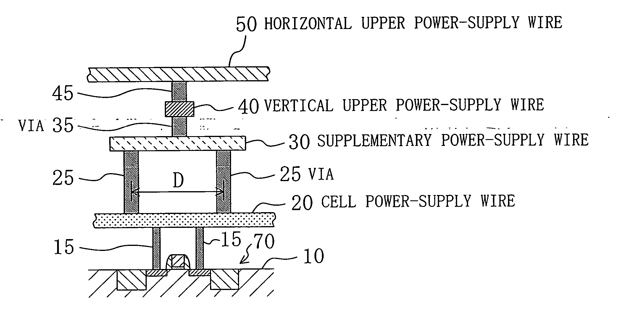
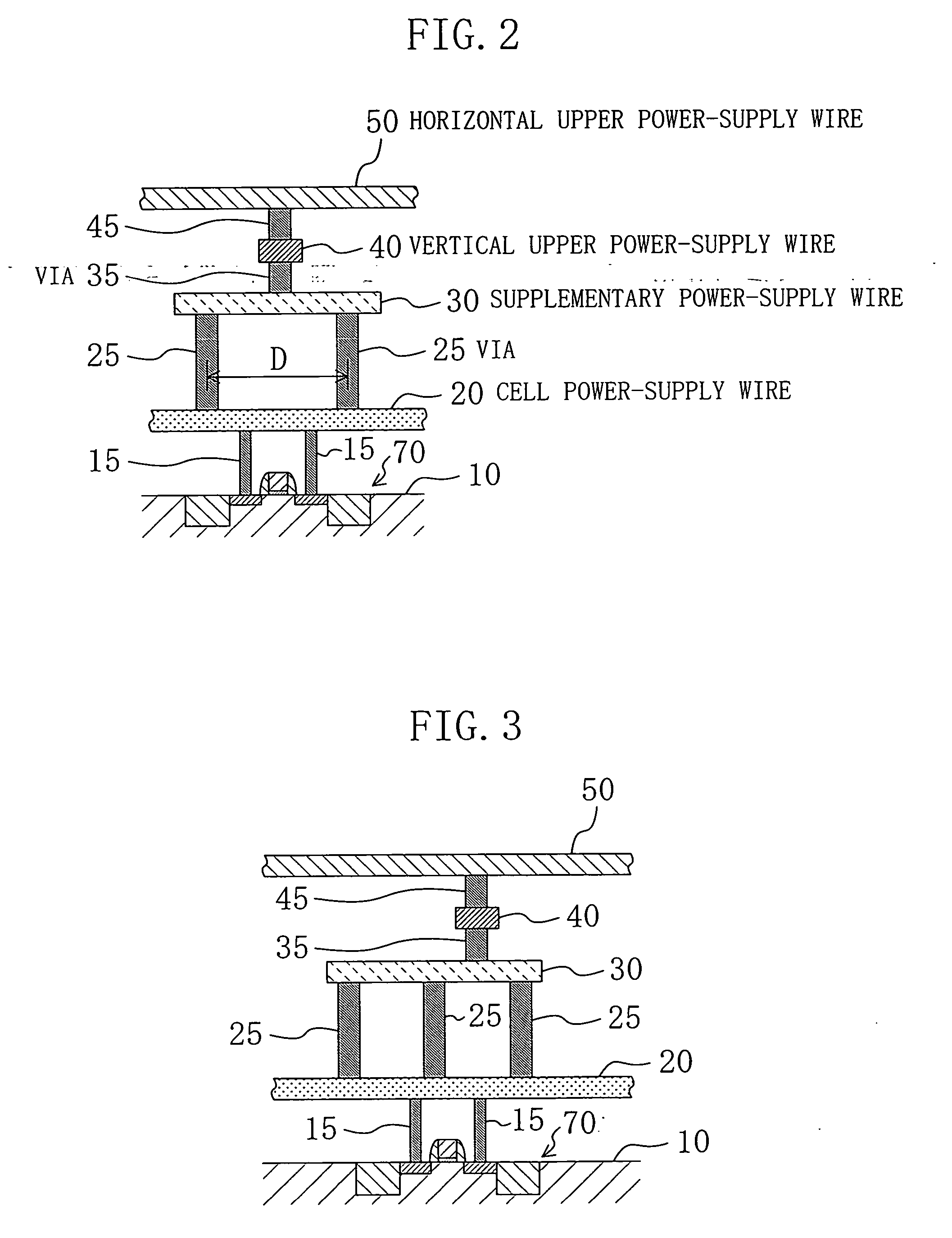
[0045]FIGS. 1 and 2 illustrate a power-supply wiring structure in a semiconductor integrated circuit according to a first embodiment of the present invention.

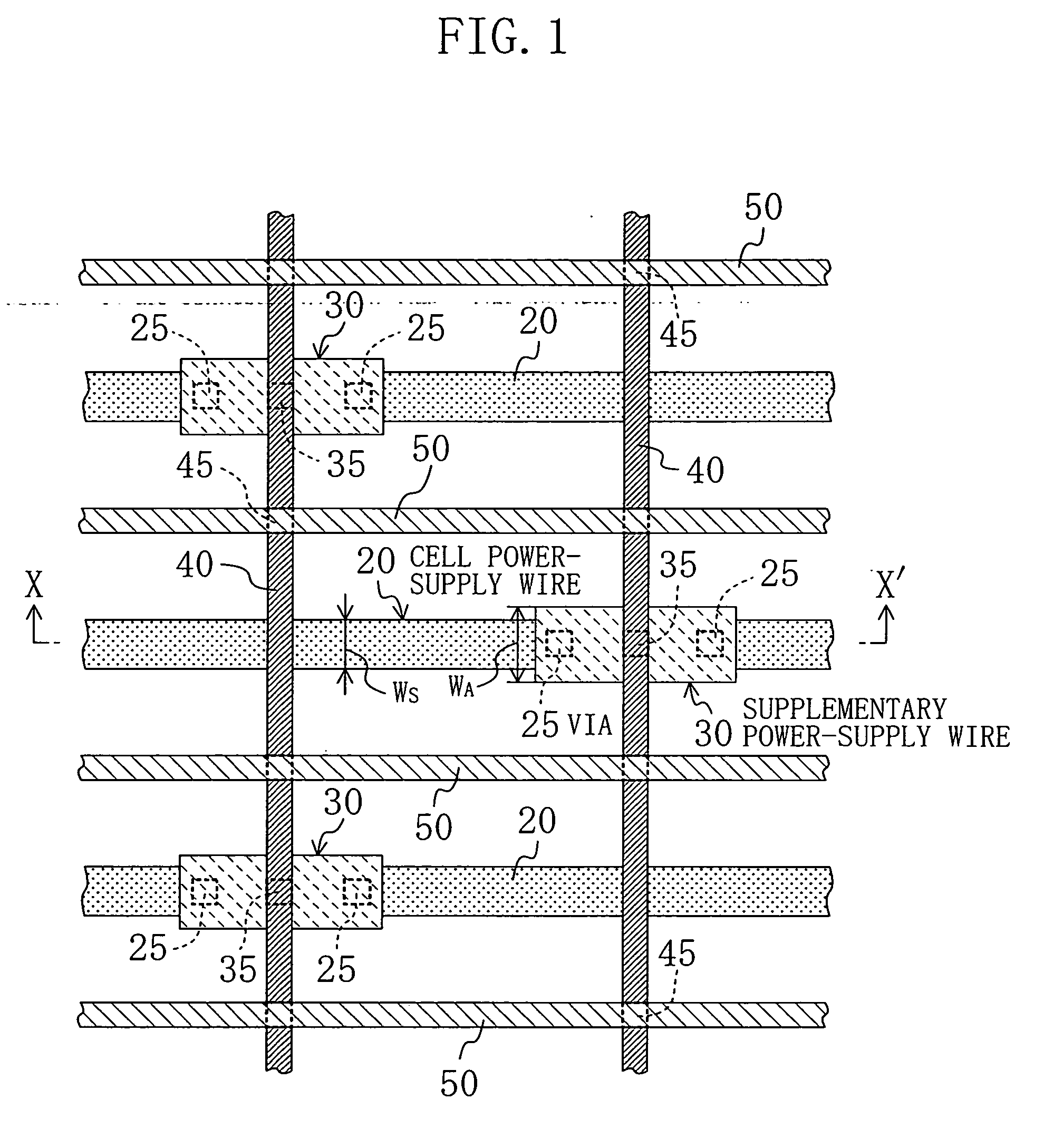
[0046]FIG. 1 is a plan view of the power-supply wiring structure in the semiconductor integrated circuit. In FIG. 1, a plurality of horizontal upper power-supply wires 50, which are disposed in the horizontal direction, and a plurality of vertical upper power-supply wires 40, which are vertically disposed below the power-supply wires 50, cross each other to form a lattice as a whole. At each of their intersection points, the horizontal power-supply wires 50 and the vertical power-supply wires 40 are connected to each other by a via 45. It should be noted that the number of vias 45 used for the connection at each intersection point is not limited to one, but two or more vias 45 may be used.

[0047] As shown in enlarged dimension in FIG. 7 (but not shown in FIG. 1), below the lattice of the upper power-supply wires 50 and 40, a p...

second embodiment

[0059]FIG. 6 illustrates a power-supply wiring structure in a semiconductor integrated circuit according to a second embodiment of the present invention.

[0060] In FIG. 6, a number of horizontal upper power-supply wires 50 and a number of vertical power-supply wires 40, which are located below the horizontal upper power-supply wires 50, are provided and connected with each other at their intersection points by vias 45 so as to form a lattice-shaped power-supply wiring structure in a wide area. Supplementary power-supply wires 30 are connected to the vertical power-supply wires 40 by vias 35, wherein the number of vias 35 provided for the connection of each supplementary power-supply wire 30 is one.

[0061] Therefore, in this embodiment, when power is supplied from the upper power-supply wires 50 and 40, the amount of IR drop can be effectively restricted below a given value.

[0062] In FIG. 6, a plurality of cell ground wires 80 are disposed so that standard cells arranged in the same...

third embodiment

[0063]FIG. 7 illustrates a power-supply wiring structure in a semiconductor integrated circuit according to a third embodiment of the present invention.

[0064] The power-supply wiring structure shown in FIG. 7 is an enlarged detail view of a main part of the power-supply wiring structure of FIG. 6 surrounded by the dotted lines.

[0065] A main feature of the semiconductor integrated circuit of this embodiment is that a given distance D between two vias 25 and 25 provided for connection of a supplementary power-supply wire 30 and a cell power-supply wire 20 located below the supplementary power-supply wire 30 is determined by the number of standard cells disposed within the given distance D. As shown in FIG. 7, in this embodiment, two standard cells 60 are horizontally disposed between the two vias 25 and 25 that connect the supplementary power-supply wire 30 and the cell power-supply wire 20.

[0066] Specifically, within the cells 60, a number of semiconductor devices 70, which contri...


PUM


Abstract

In a semiconductor integrated circuit including a plurality of cells, a supplementary power-supply wire is disposed between a lattice-shaped upper power-supply wire and a lower cell power-supply wire for cases in which power is supplied from the upper power-supply wire to the lower cell power-supply wire. The supplementary power-supply wire and the lower cell power-supply wire are connected by two vias. The supplementary power-supply wire and the upper power-supply wire are connected by a single via. Current from the supplementary power-supply wire is divided by the two vias and then supplied to the lower cell power-supply wire. Therefore, when power is supplied from the upper power-supply wire to the lower cell power-supply wire, current concentration at the connection points of the lower cell power-supply wire to the vias is decreased, thereby reducing wire breaks caused by EM (electro migration).

Description

CROSS-REFERENCE TO RELATED APPLICATIONS [0001] This Non-provisional application claims priority under 35 U.S.C. §119(a) on Patent Application No. 2004-286576 filed in Japan on Sep. 30, 2004, the entire contents of which are incorporated herein by reference. BACKGROUND OF THE INVENTION [0002] The present invention relates to semiconductor integrated circuits, and more particularly relates to a power-supply wiring structure for optimizing the amount of IR drop and the flow of current in the power-supply wiring. [0003] As semiconductor devices for semiconductor integrated circuits have been miniscaled, the number of semiconductor devices integrated on a chip has been increasing year after year, forcing the power-supply wiring in the chip to be increased in length and decreased in wire width. In addition, the problem of how to ensure signal integrity has manifested itself. In particular, how to deal with IR drop and electro migration (which will be hereinafter referred to as “EM”) that ...

Claims


Application Information

Patent Timeline
Patent Type & Authority Applications(United States)
IPC IPC(8): H01L21/4763H01L23/52
CPCH01L21/76838H01L27/11807
Inventor NISHIMURA, HIDETOSHI
Owner III HLDG 12 LLC
Why Eureka
Try Eureka