Technology dependent transformations for CMOS in digital design synthesis

a technology of digital design and transformation, applied in the field of technology dependent cmos transistor level transformation, can solve the problems of reducing the realistic overall questionable improvement to meet timing, size or power, etc., and achieves the effect of reducing cross-coupling, realizing improvement of such an approach, and lowering interconnected delay

Inactive Publication Date: 2006-04-06
RANA AMAR PAL SINGH +1
View PDF4 Cites 14 Cited by
  • Summary
  • Abstract
  • Description
  • Claims
  • Application Information

AI Technical Summary

Problems solved by technology

The realistic improvement of such an approach is considerably diminished in each of the automated steps for not being fully capable to match the manual optimizations due to algorithmic deficiencies, unacceptable CPU run time and memory needed during: the input design specification technology independent logic minimization stage, transistor level stages clustering, transistor sizing algorithms, local automated dynamic precharge and evaluation clock generation at the high frequencies needed and automated layout of dynamic clusters and subsequent placement and routing of such dynamic clusters having widely differing aspect ratios with the rest of standard cells for CMOS ASIC design resulting in overall questionable improvement to meet timing, size or power constraints.

Method used


Image

  • Technology dependent transformations for CMOS in digital design synthesis
  • Technology dependent transformations for CMOS in digital design synthesis
  • Technology dependent transformations for CMOS in digital design synthesis

Examples


Embodiment Construction

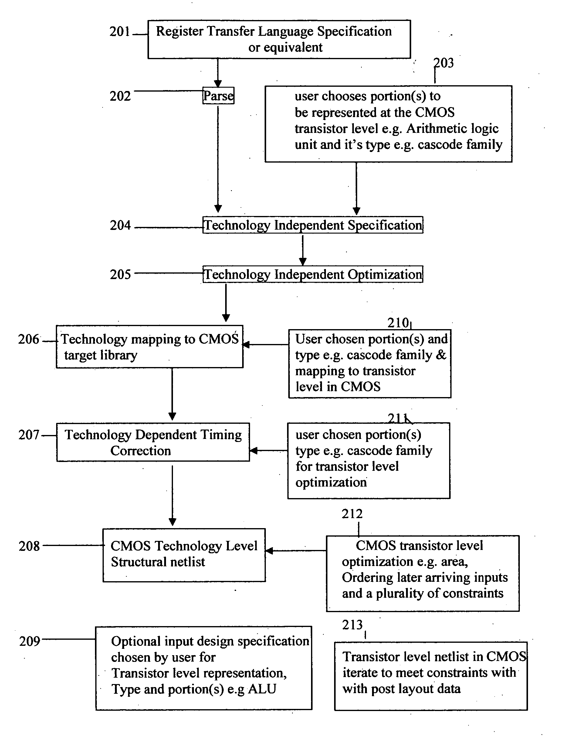
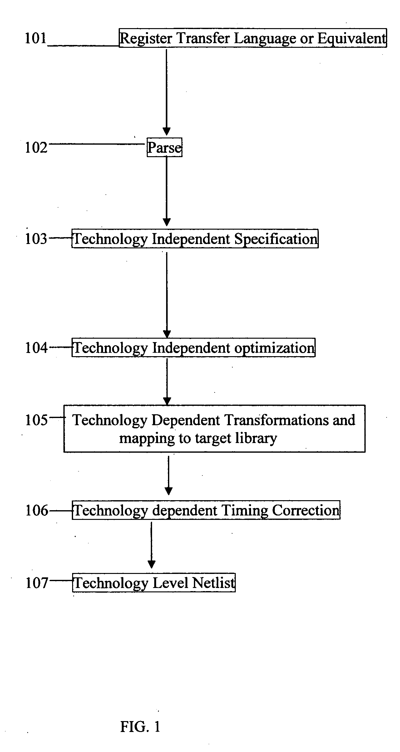
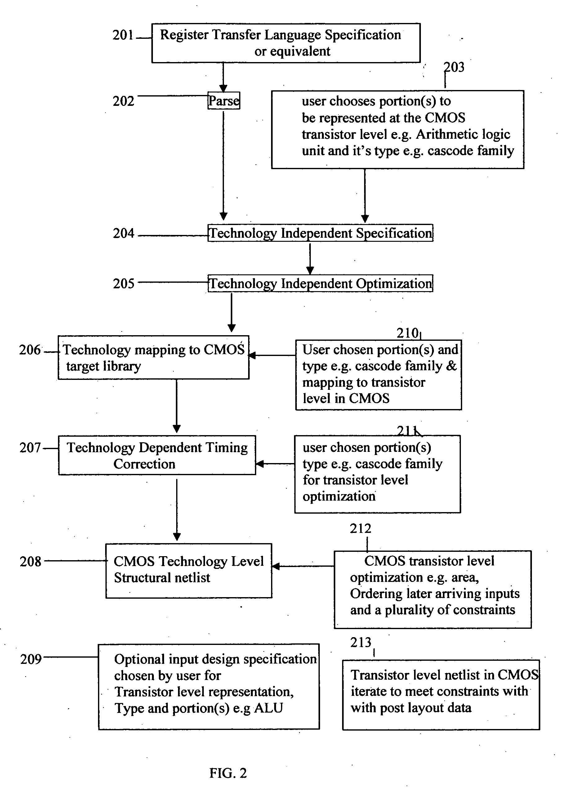
[0044] The present invention pertains to automated technology dependent transformations for CMOS digital design synthesis resulting in a combination of CMOS interconnected standard-cells from a target CMOS library being mapped and transistor-level representation for all or portion of the input design specification, the transistor level type and portion or portions to be represented at the transistor level representation being chosen by a user, transistor sizing and evaluating the combination of said transistor-level representation and standard-cell mapping iteratively to meet delay, size and power constraints for CMOS.

[0045] The present invention pertains to technology dependent transformations capable of creation and optimization of CMOS complex functional blocks, hereinafter designated design-specific cells. A fuller understanding of the overall organization of an IC design process using CMOS design-specific cells created in accordance with the present invention for designing hig...


PUM


Abstract

The present invention pertains to automated technology dependent transformations for CMOS digital design synthesis resulting in a combination of CMOS interconnected standard-cells from a target CMOS library being mapped and transistor-level representation for all or portion of the input design specification, the transistor level type and portion or portions to be represented at the transistor level representation being chosen by a user, transistor sizing and evaluating the combination of said transistor-level representation and standard-cell mapping iteratively to meet delay, size and power constraints for CMOS.

Description

[0001] CROSS-REFERENCE TO RELATED APPLICATIONS [0002] This is a divisional application of parent utility application Ser. No. 10 / 172,448 filed on Jun. 17, 2002 by the same inventors, filed pursuant to election, based on the office action of May 14, 2004, such parent application has been allowed and is in the issue process for the elected species, transformations for Silicon-On-Insulator (SOI) ICs, while this divisional application is for the unelected species, transformations for CMOS ICs, of the parent application, assigned to Group Art Unit 2825 with Examiner Stacy A. Whitmore. BACKGROUND OF THE INVENTION [0003] 1. Technical Field [0004] The invention relates to technology dependent transformations for design automation and more particularly to technology dependent CMOS transistor level transformations where user specifies the portion or portions to be represented at the transistor level and the transistor level type e.g. cascode family, NORA logic etc. [0005] 2. Glossary of Terms...

Claims


Application Information

Patent Timeline
Patent Type & Authority Applications(United States)
IPC IPC(8): G06F17/50
CPCG06F17/5045G06F30/30
Inventor RANA, AMAR PAL SINGHSINGH, NIRMAL
Owner RANA AMAR PAL SINGH
Why Eureka
Try Eureka