Circuits and manufacturing configurations of compact band-pass filter

a band-pass filter and manufacturing configuration technology, applied in the field of device configuration and process for manufacturing compact band-pass filters, can solve the problems of limited form factor and circuit size reduction, the configuration and the process of manufacturing the band-pass filter (bpf) are still faced with technical challenges, and people of ordinary skill in the art still have difficulties to satisfy such demands, so as to achieve the effect of reducing the height and size, simplifying the manufacturing process, and increasing the reliability of the devi

Inactive Publication Date: 2006-04-13
CYNTEC
View PDF18 Cites 14 Cited by
  • Summary
  • Abstract
  • Description
  • Claims
  • Application Information

AI Technical Summary

Benefits of technology

[0011] It is therefore an object of the present invention to provide a new structural configuration and manufacture method for manufacturing an bandpass filter (BPF) with simplified manufacturing processes to produce BPF with improved form factors h...

Problems solved by technology

For those of ordinary skill in the art, the configurations and the processes of manufacturing the band-pass filters (BPF) are still faced with technical challenges due to the fact that noises and harmonic resonance signals of higher and lower frequencies cannot be effectively filtered out.
Furthermore, there are limitations to further improve the form factor and to reduce the size of the BPF circuits due to a conventional configuration by assembling and packaging the BPF by using different circuit components, e.g., circuit components of capacitors and inductors.
Due to conventional method and configurations of assembling electronic components into BPF, a person of ordinary skill in the art still have difficulties to satisfy such demands due to these technical limitations.
Such BPF occupies large areas thus greatly limiting the flexibilities for miniaturization.
The conventional BPFs as shown still have the limitations that there are spurious signals passing through at the low frequencies and resonant harmonic noises at higher frequencies.
Sasaki's technique however is limited by the larger si...

Method used


Image

  • Circuits and manufacturing configurations of compact band-pass filter
  • Circuits and manufacturing configurations of compact band-pass filter
  • Circuits and manufacturing configurations of compact band-pass filter

Examples


Embodiment Construction

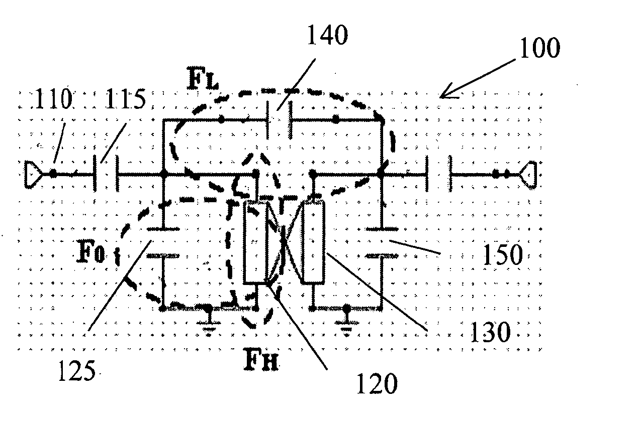
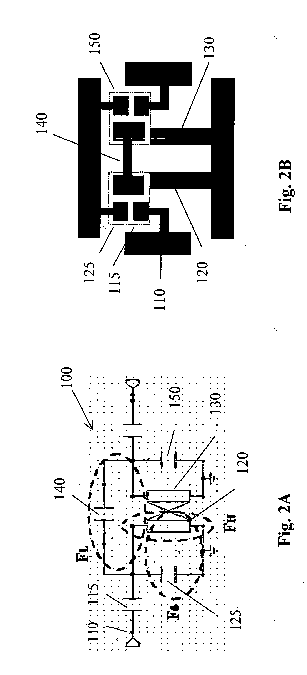
[0031]FIG. 2A shows a circuit diagram of a bandpass filter 100 and FIG. 2B is a top view of the micro-strip implementation supported on a substrate 105 of this invention implemented as a semi-lump distributed circuit by a micro-strip line or strip line configuration as that shown in FIG. 2B. The micro-strip 120 is serial connected to the input line 110 with a serially connected capacitor 115 to generate a high frequency resonance fH. The micro-strip 120 connected in parallel to a capacitor 125 to generate a resonance frequency at a transmission frequency f0. The micro-strip 120 combined with a coupled micro-strip 130 with a another capacitor 140 connected in parallel that in combination with an external feedback capacitor 150 to generate a low frequency resonance at a low frequency fL. The BPF 100 is configured as a low frequency depression BPF for transmitting a band-pass signal with a depressed low frequency with reduced low frequency noises.

[0032] Referring to FIGS. 2C-1 to 2C-1...


PUM


Abstract

A filter circuit that includes a thin film layer supported on a substrate serving as a medium layer for a capacitor formed between a top electrode layer and a bottom electrode layer formed above and below the thin film layer. The top electrode layer is patterned into microstrips for functioning as an inductor for the filter circuit.

Description

BACKGROUND OF THE INVENTION [0001] 1. Field of the Invention [0002] This invention relates generally to the device configuration and processes for manufacturing band-pass filters (BPF). More particularly, this invention relates to an improved circuit and packaging configuration and manufacturing process for making compact band-pass filters. [0003] 2. Description of the Prior Art [0004] For those of ordinary skill in the art, the configurations and the processes of manufacturing the band-pass filters (BPF) are still faced with technical challenges due to the fact that noises and harmonic resonance signals of higher and lower frequencies cannot be effectively filtered out. Furthermore, there are limitations to further improve the form factor and to reduce the size of the BPF circuits due to a conventional configuration by assembling and packaging the BPF by using different circuit components, e.g., circuit components of capacitors and inductors. As more and more mobile communication d...

Claims


Application Information

Patent Timeline
IPC IPC(8): H01P1/203
CPCH01P1/20381
Inventor WANG, CHUNG-HSIUNGWANG, KENG-HONG
Owner CYNTEC
Why Eureka
Try Eureka