Thin film transistor array plate, liquid crystal display panel and method of preventing electrostatic discharge

Inactive Publication Date: 2006-04-13
CHUNGHWA PICTURE TUBES LTD
View PDF10 Cites 40 Cited by
  • Summary
  • Abstract
  • Description
  • Claims
  • Application Information

AI Technical Summary

Benefits of technology

[0009] Accordingly, the present invention is directed to a thin film transistor array plate that utilizes the original testing

Problems solved by technology

Although the conventional display such as cathode ray tube (CRT) has superior display quality and relatively cheap to procure, the electron gun structure within the CRT renders it bulky, heavy and power hungry.
Moreover, radiation harmful to the eyes may also be produced.
Furthermore, external factors such as transportation or changes in the environment may lead to the accumulation of some static electric charges in the liquid crystal display panel.
When the accumulation of static charges exceed a definite amount

Method used


Image

  • Thin film transistor array plate, liquid crystal display panel and method of preventing electrostatic discharge
  • Thin film transistor array plate, liquid crystal display panel and method of preventing electrostatic discharge
  • Thin film transistor array plate, liquid crystal display panel and method of preventing electrostatic discharge

Examples


Embodiment Construction

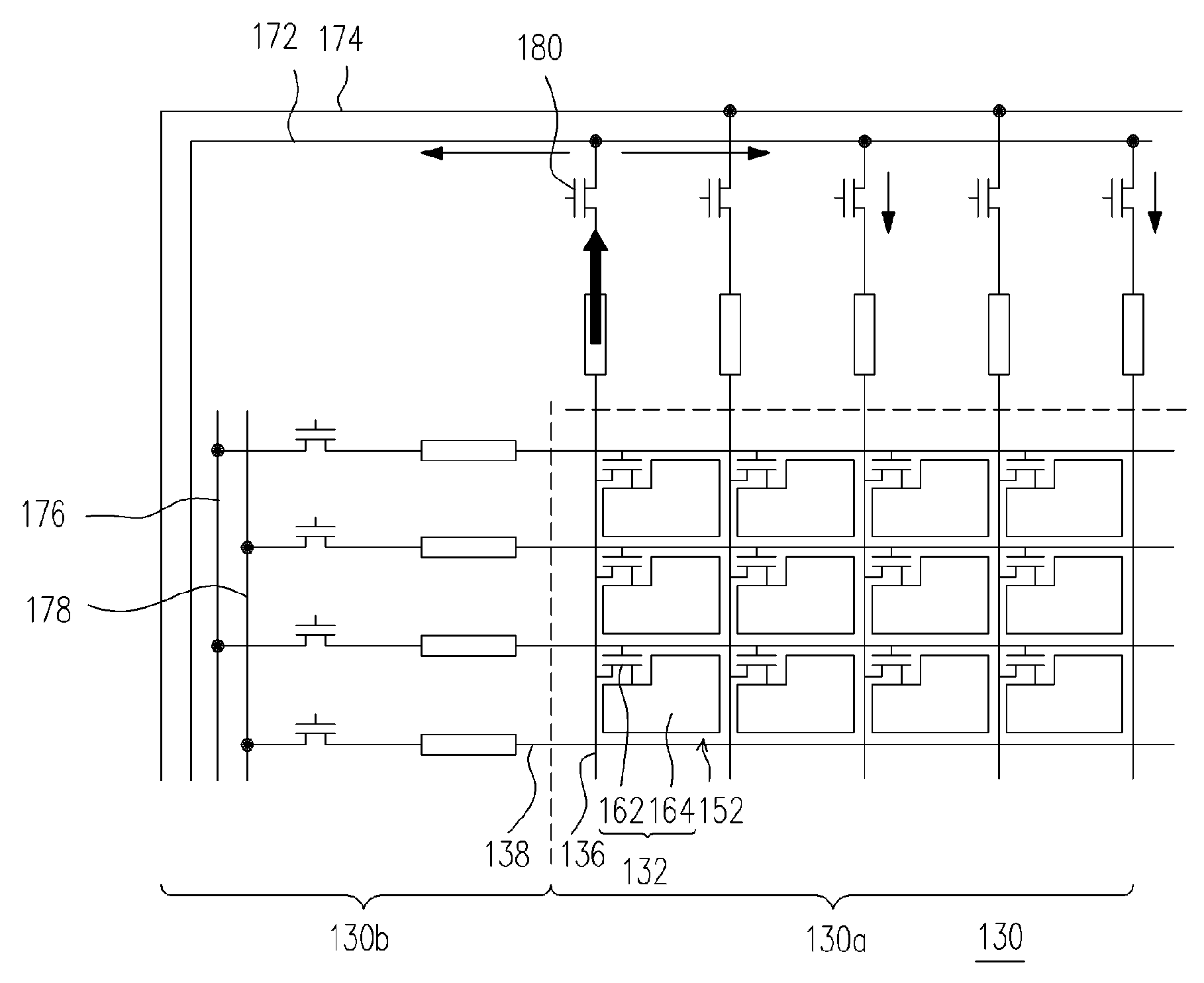
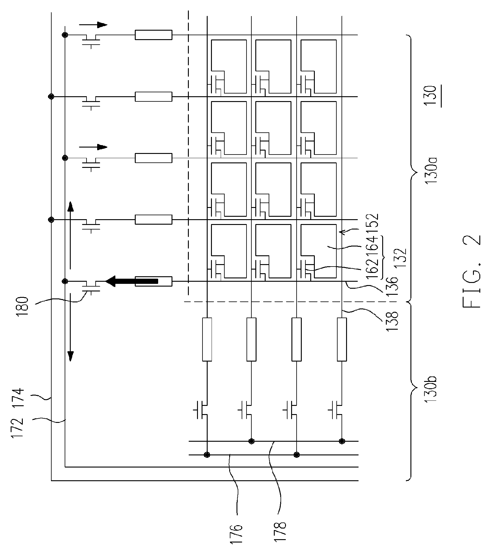
[0022] Reference will now be made in detail to the present preferred embodiments of the invention, examples of which are illustrated in the accompanying drawings. Wherever possible, the same reference numbers are used in the drawings and the description to refer to the same or like parts.

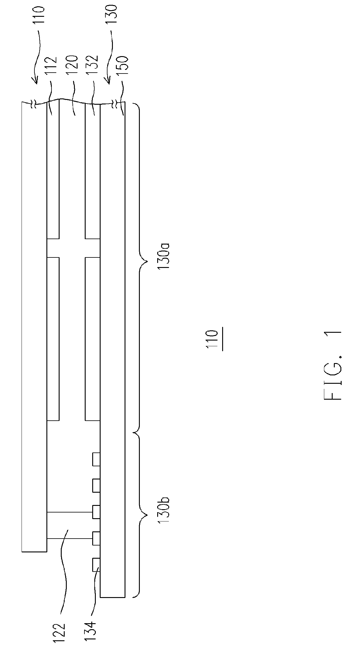
[0023]FIG. 1 is a sectional view showing part of a liquid crystal display panel according to one embodiment of the present invention. To simplify FIG. 1, only relevant components are sketched. The liquid crystal display panel 100 in FIG. 1 comprises a color filter plate 110, a liquid crystal layer 120 and a thin film transistor array plate 130. The color filter plate 110 and the thin film transistor array plate 130 are joined together through a sealant 122. The liquid crystal layer 120 is disposed within the space bounded by the color filter plate 110, the thin film transistor array plate 130 and the sealant 122. In addition, the color filter plate 110 comprises several color filter patterns 112. T...


PUM


Abstract

A thin film transistor array plate, a liquid crystal display panel and a method of preventing electrostatic discharge thereof are provided. The thin film transistor array comprises a substrate, pixel structures, switching devices, lead lines and electrostatic discharge (ESD) protecting circuits. The substrate has a display region and a peripheral circuit region. The pixel structures are disposed within the display region and the switching devices are disposed within the peripheral circuit region. The lead lines are disposed on the substrate to electrically connect the pixel structures and the switching devices. The ESD protecting circuits are disposed within the peripheral circuit region such that each ESD protecting circuit is electrically connected to the corresponding switching devices. The ESD protecting circuits prevent electrostatic discharge, simplify the circuit layout and improve production efficiency of the plate and the panel.

Description

BACKGROUND OF THE INVENTION [0001] 1. Field of the Invention [0002] The present invention generally relates to a device array plate, a display panel and a method of preventing electrostatic discharge. More particularly, the present invention relates to a thin film transistor array plate, a liquid crystal display panel and a method of preventing electrostatic discharge. [0003] 2. Description of Related Art [0004] Through the rapid development of multi-media technologies, image data are now transmitted mostly in a digital format instead of an analogue format. To fit the life style of modern people, video or image devices have an increasingly light and compact design. Although the conventional display such as cathode ray tube (CRT) has superior display quality and relatively cheap to procure, the electron gun structure within the CRT renders it bulky, heavy and power hungry. Moreover, radiation harmful to the eyes may also be produced. With big leaps in the techniques of manufacturing ...

Claims


Application Information

Patent Timeline
IPC IPC(8): G09G3/36
CPCG02F1/136204Y10S345/904
Inventor CHOU, JUI-YUANYU, CHIH-LUNGHO, CHIEN-KUO
Owner CHUNGHWA PICTURE TUBES LTD
Why Eureka
Try Eureka