
Method for improving programming speed in memory devices

a memory device and programming speed technology, applied in the field of memory devices, can solve problems such as low efficiency of programming or erasing operations

Active Publication Date: 2006-04-13
MEMORY TECHNOLOGIES LLC
View PDF10 Cites 2 Cited by
  • Summary
  • Abstract
  • Description
  • Claims
  • Application Information

AI Technical Summary

Benefits of technology

[0006] Thus, the first aspect of the present invention provides a method for improving efficiency in performing a data change in a memory section in a memory device by applying a voltage to the memory device in a time period, the time period comprising a first time segment for data setup and a second time segment following the first time segment, and wherein the applied voltage must reach a predetermined voltage value in the second time segment for effecting the data change. The method comprises: providing the applied voltage to the memory device such that the applied voltage substantially reaches the predetermined voltage value also in at least a part of the first time segment.

Problems solved by technology

However, its I / O interface allows only sequential access of data.
As such, the programming or erasing operation is not highly efficient.

Method used


Image

  • Method for improving programming speed in memory devices
  • Method for improving programming speed in memory devices
  • Method for improving programming speed in memory devices

Examples


Embodiment Construction

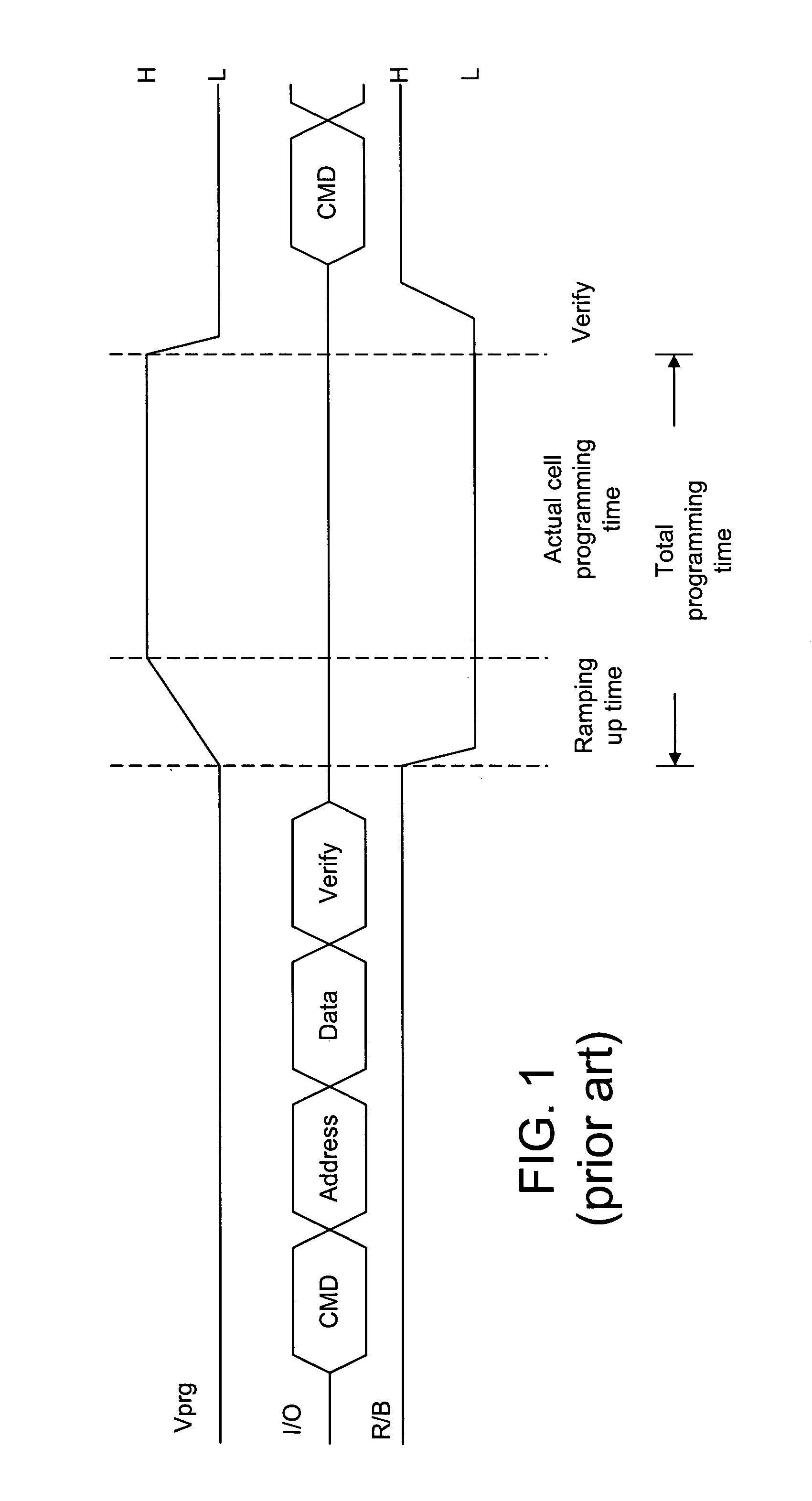
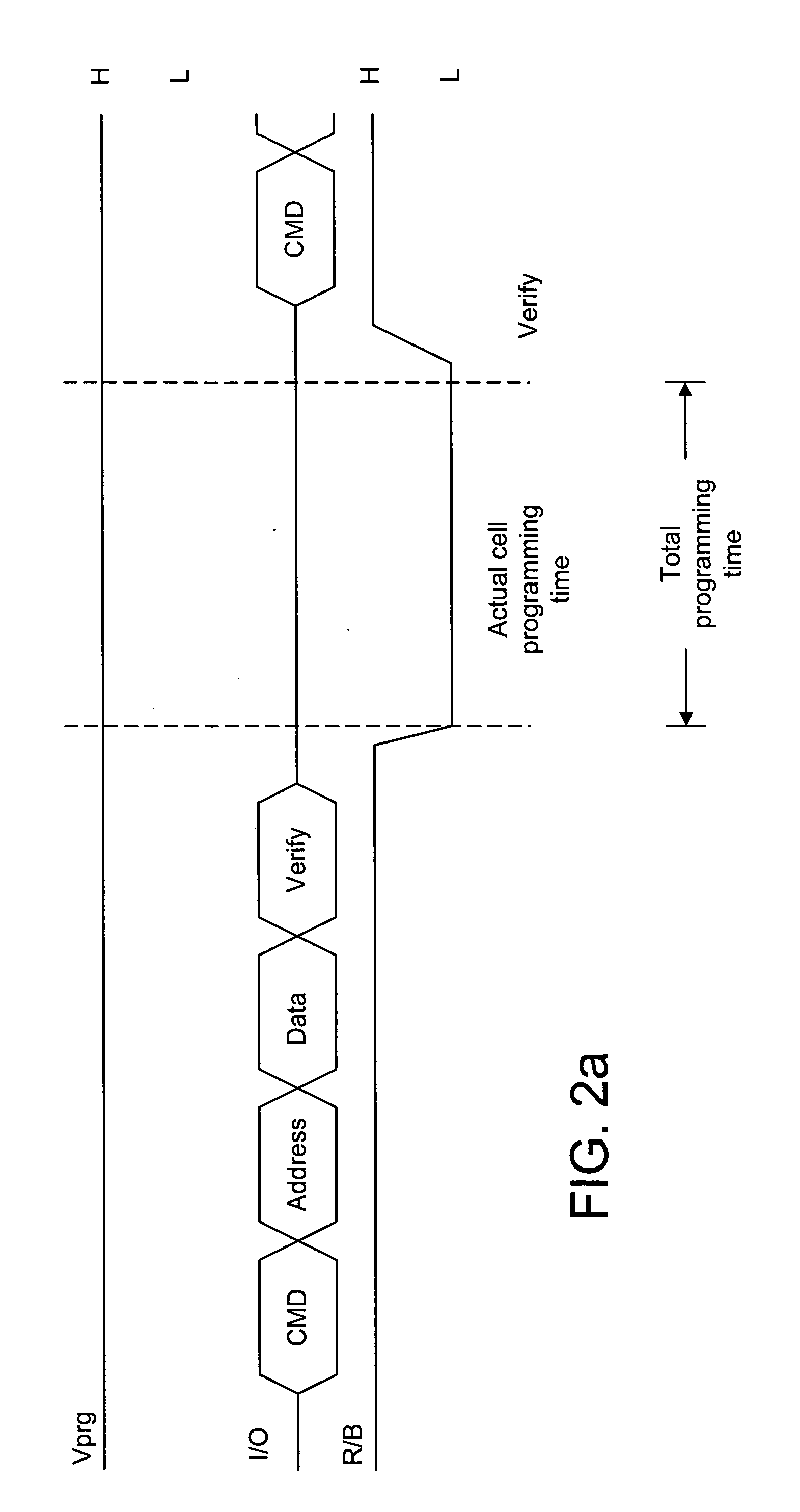
[0062] In order to improve the efficiency in programming or erasing a memory device, it is possible to eliminate the ramping up time in the programming / erasing operation. According to the present invention, the programming / erasing voltage, Vprg, can be kept “high” all the time, as shown in FIG. 2a. As such, actual cell programming starts as soon as the R / B signal drops to the low state. As a result, the total programming time is essentially equal to the actual cell programming time.

[0063] In another embodiment of the present invention, Vprg is ramped up during the I / O setup period. For example, it is possible to start ramping up the programming / erasing voltage Vprg right after the command (CMD) for program / erase is received, as shown in FIG. 2b. Thus, Vprg can be ramped up during the I / O setup period, so long as Vprg becomes “H” before the R / B signal drops to the low state.

[0064] In yet another embodiment of the present invention, Vprg is ramped up during the I / O setup period to b...


PUM


Abstract

A high voltage up to 20V is usually applied to a NAND flash memory device for programming or easing a memory section. The programming / easing voltage must reach that high voltage state when the R / B signal is in the L state to start the actual cell programming or erasing. To improve the programming or erasing efficiency, the applied voltage also reaches the high voltage state before the R / B signal is set from H to L. The memory device may have one connecting pad to receive a normal operating voltage and another connection pad to receive the programming and erasing voltage. The EXT_CSD register may have a mode bit to indicate whether the memory device supports the programming and erasing operation.

Description

FIELD OF THE INVENTION [0001] The present invention relates generally to a memory device and, more particularly, to the programming of such device. BACKGROUND OF THE INVENTION [0002] Flash memory is a form of EEPROM (Electronically Erasable Programmable Read Only Memory) that allows multiple memory locations to be erased or written in one programming operation. Flash memory is a transistor technology and is generally classified into NOR flash and NAND flash. The names refer to the gate logic architecture of the memory cells. NOR flash memory has a longer erase and Write times than NAND flash memory, but NOR flash memory has a full address / data interface that allows random access to any location. NOR is suitable for storage of program code that needs to be infrequently updated, as in digital cameras and PDAs. [0003] NAND flash memory has faster erase and write times (per bytes, depending on the access), higher density and lower cost per bit than NOR flash. However, its I / O interface ...

Claims


Application Information

Patent Timeline
IPC IPC(8): G11C16/04
CPCG11C16/12G11C16/30
Inventor MYLLY, KIMMO
Owner MEMORY TECHNOLOGIES LLC
Features
  • Generate Ideas
  • Intellectual Property
  • Life Sciences
  • Materials
  • Tech Scout
  • Unparalleled Data Quality
  • Higher Quality Content
  • 60% Fewer Hallucinations
Learn More