

Silicon wafer laser processing method and laser beam processing machine
a laser processing and laser technology, applied in laser beam welding apparatus, manufacturing tools, welding/soldering/cutting articles, etc., can solve the problems of reducing productivity, difficult to smoothly divide silicon wafer along the dividing line, etc., to achieve efficient deterioration of the inside layer of silicon wafer and high silicon wafer permeability
- Summary
- Abstract
- Description
- Claims
- Application Information
AI Technical Summary
Benefits of technology
Problems solved by technology
Method used
Image

Examples
experimental example 1
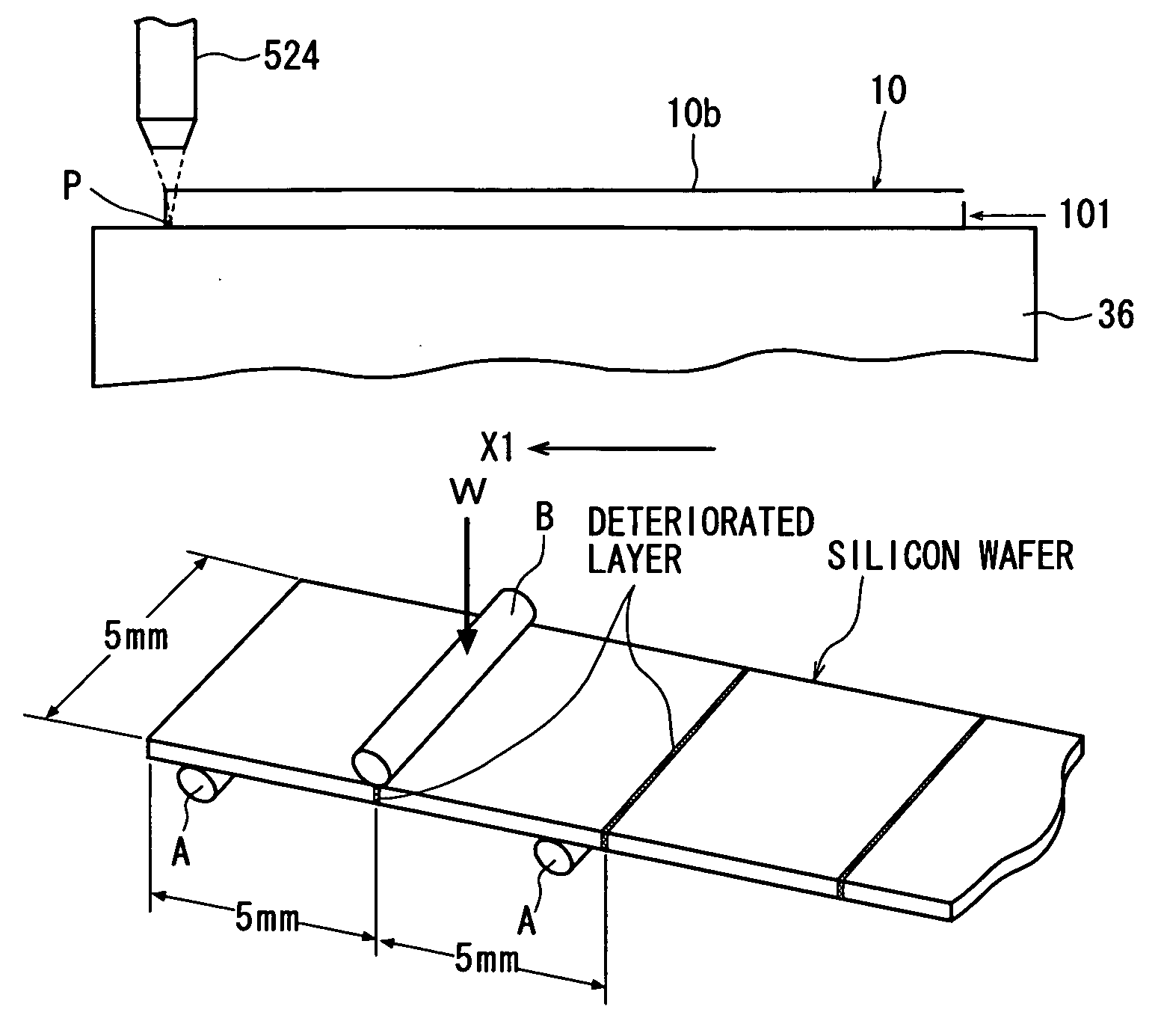
[0037] Dividing lines were formed at intervals of 5 mm in a lattice pattern on a silicon wafer having a diameter of 200 mm and a thickness of 600 μm, and laser processing was carried out along the dividing lines under the following processing conditions by using a pulse laser beam having a wavelength of 1,064 nm to form a deteriorated layer in the inside of the silicon wafer along the dividing lines. One deteriorated layer had a thickness of about 50 μm, and 12 layers formed from this deteriorated layer were formed so that they were exposed to both surfaces of the silicon wafer. [0038] light source: LD excited Q switch Nd:YVO4 laser [0039] wavelength: pulse laser beam having a wavelength of 1,064 nm [0040] repetition frequency: 40 kHz [0041] pulse width: 20 ns [0042] average output: 4 W [0043] focusing spot diameter: 1.0 μm [0044] processing-feed rate: 40 mm / sec
[0045] The silicon wafer having a deteriorated layer that was formed along the dividing lines under the above processing c...
experimental example 2
[0047] Dividing lines were formed at intervals of 5 mm in a lattice pattern on a silicon wafer having a diameter of 200 mm and a thickness of 600 μm, and laser processing was carried out along the dividing lines under the following processing conditions by using a pulse laser beam having a wavelength of 1,340 nm to form a deteriorated layer in the inside of the silicon wafer along the dividing lines. One deteriorated layer had a thickness of about 50 μm like the above Experimental Example 1, and 12 layers formed from this deteriorated layer were formed so that they were exposed to both surfaces of the silicon wafer. [0048] light source: LD excited Q switch Nd:YVO4 laser [0049] wavelength: pulse laser beam having a wavelength of 1,340 nm [0050] repetition frequency: 40 kHz [0051] pulse width: 20 ns [0052] average output: 4 W [0053] focusing spot diameter: 1.3 μm [0054] processing-feed rate: 40 mm / sec
[0055] The silicon wafer having a deteriorated layer that was formed along the divid...
experimental example 3
[0056] Dividing lines were formed in a lattice pattern on a silicon wafer having a diameter of 200 mm and a thickness of 600 μm at intervals of 5 mm, and laser processing was carried out along the dividing lines under the following processing conditions by using a pulse laser beam having a wavelength of 1,550 nm to form a deteriorated layer in the inside of the silicon wafer along the dividing lines. One deteriorated layer had a thickness of about 50 μm like the above Experimental Examples 1 and 2, and 12 layers formed from this deteriorated layer were formed so that they were exposed to both surfaces of the silicon wafer. [0057] light source: LD excited Q switch Nd:YVO4 laser [0058] wavelength: pulse laser beam having a wavelength of 1,550 nm [0059] repetition frequency: 40 kHz [0060] pulse width: 20 ns [0061] average output: 4 W [0062] focusing spot diameter: 1.5 μm [0063] processing-feed rate: 40 mm / sec
[0064] The silicon wafer having a deteriorated layer that was formed along th...
PUM
| Property | Measurement | Unit |
|---|---|---|
| Wavelength | aaaaa | aaaaa |
| Wavelength | aaaaa | aaaaa |
Abstract
Description
Claims
Application Information