Sol-Gel method and method for manufacturing optical crystal fiber using the same

a technology of optical crystal fiber and gel, which is applied in the field of manufacturing optical fiber preforms and optical crystal fibers, can solve the problems of reducing the purity of silica glass of polymeric organic substances having c backbone structure, mixing sol is subjected to a very large stress, and the purity of silica glass is reduced. , to achieve the effect of preventing the decrease of coupling force, minimizing the contamination of sol gel, and improving gel consolidation

Inactive Publication Date: 2006-04-20
SAMSUNG ELECTRONICS CO LTD
View PDF5 Cites 3 Cited by
  • Summary
  • Abstract
  • Description
  • Claims
  • Application Information

AI Technical Summary

Benefits of technology

[0013] One aspect of the present invention relates to a sol-gel process capable of minimizing the contamination of a sol-gel caused by remaining organic substances while preventing the decrease in the coupling force among particles of the sol-gel.
[0014] One embodiment of the present invention is directed to a sol-gel method including a dispersion step of mixing a sol having fumed silica dispersed into de-ionized water with a hydrolysis substance having an organic binder having Si—O backbone structure; a formation step of injecting the sol into a mold to form a gel; a drying step of drying the gel; a low-temperature heat treatment step of removing organic substances remaining in the gel; a chlorine treatment step of removing impurities remaining in the gel and OH radicals; and a high-temperature heat treatment step of heating the gel at a high temperature to improve the consolidation of the gel.

Problems solved by technology

The mixed sol is subjected to a very large stress during gelling and drying due to small pores.
However, conventional sol-gel processes have a problem in that polymeric organic substances having C backbone structure decrease the purity of silica glass, such as an optical fiber preform or optical crystal fiber, manufactured by the sol-gel processes.

Method used


Image

  • Sol-Gel method and method for manufacturing optical crystal fiber using the same
  • Sol-Gel method and method for manufacturing optical crystal fiber using the same
  • Sol-Gel method and method for manufacturing optical crystal fiber using the same

Examples


Embodiment Construction

[0019] Hereinafter, embodiments of the present invention will be described with reference to the accompanying drawings. For the purposes of clarity and simplicity, a detailed description of known functions and configurations incorporated herein will be omitted when it may obscure the subject matter of the present invention.

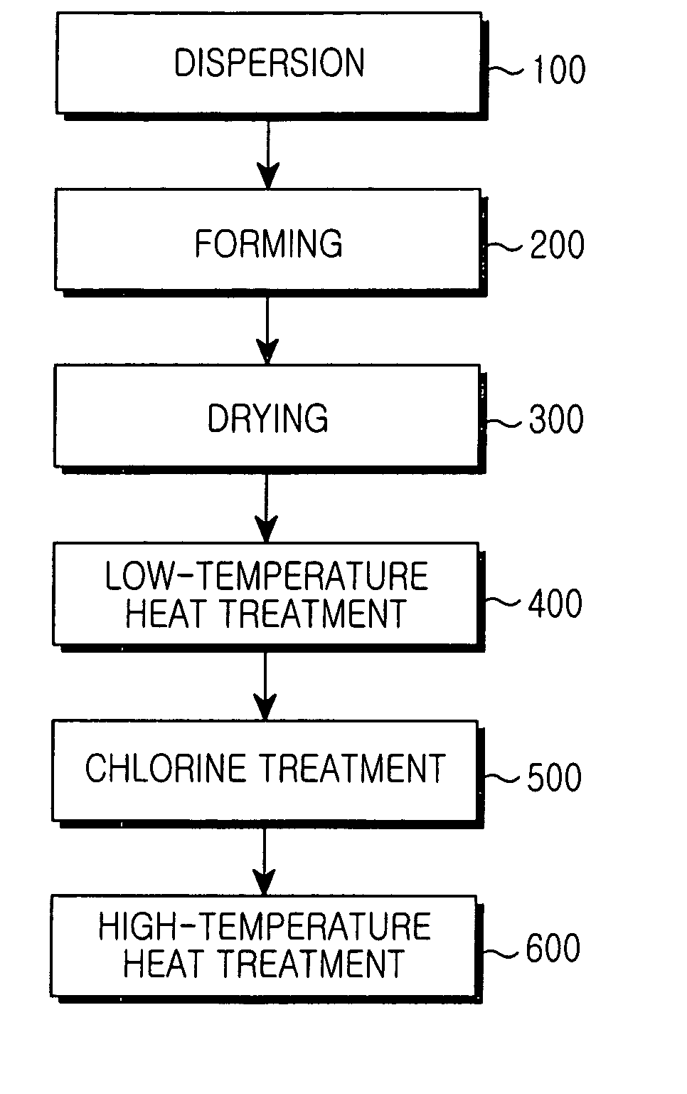
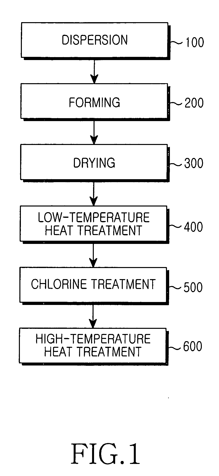
[0020]FIG. 1 is a flowchart showing steps of a sol-gel method according to an embodiment of the present invention. The method includes a dispersion step 100 of creating a sol, a forming step 200 of forming a gel by injecting the dispersed sol into a mold, a drying step 300, a low-temperature treatment step 400, a chlorine treatment step 400, and a high-temperature heat treatment step 600.

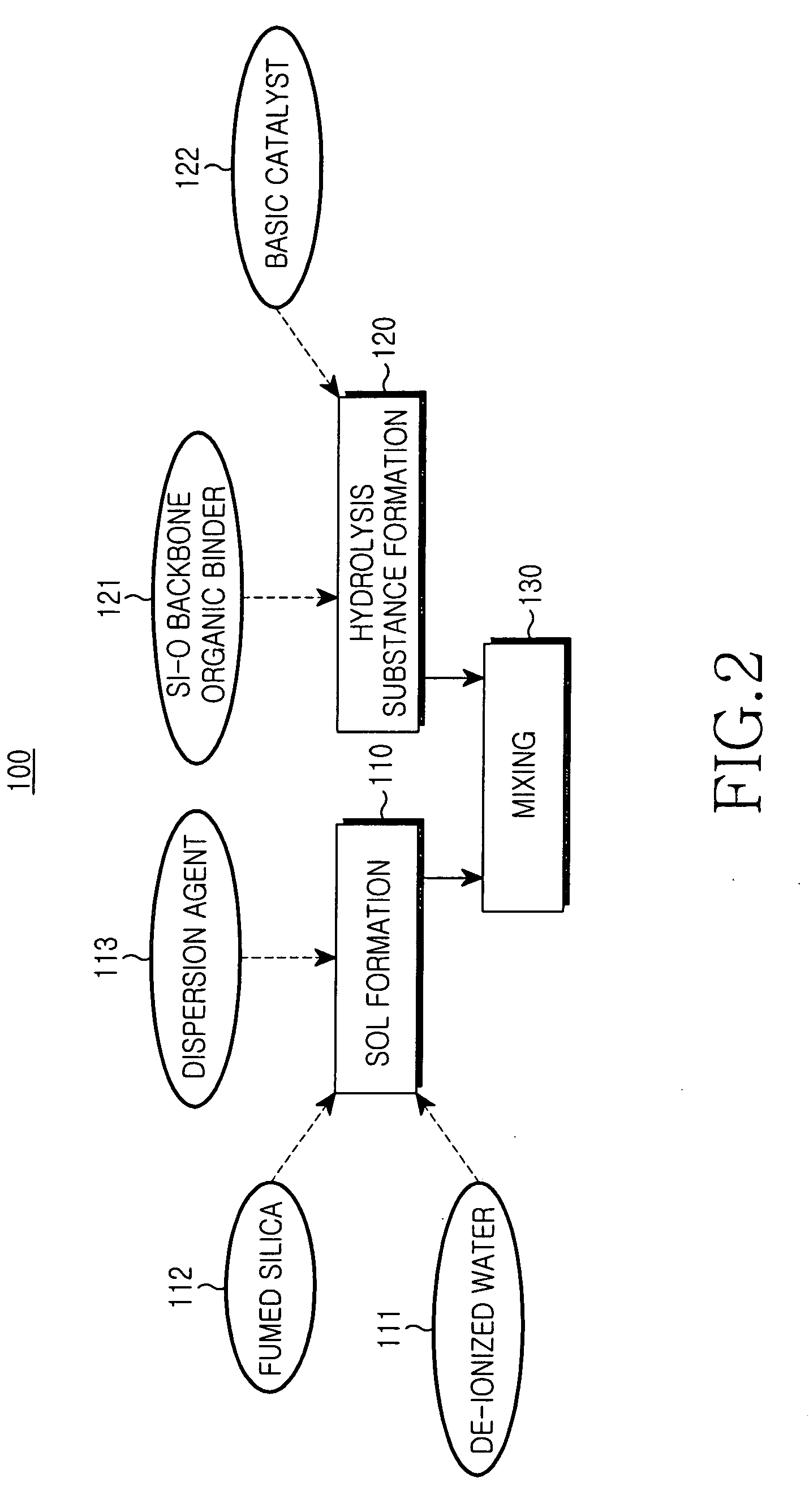
[0021]FIG. 2 is a flowchart showing sub-steps of the dispersion step 100 shown in FIG. 1. The dispersion step 100 includes a sol formation step 110 of fabricating a dispersed sol by adding fumed silica 112, a dispersion agent 113, and a plasticizer into a solution such as de-ion...


PUM

PropertyMeasurementUnit
temperatureaaaaaaaaaa

Abstract

A sol-gel process is disclosed. The process includes the steps of creating a sol by dispersing an organic binder having Si—O backbone structure into de-ionized water together with fumed silica, injecting the dispersed sol into a mold to form a gel, drying the gel, removing organic substances remaining in the gel, removing impurities remaining in the gel and OH radicals, and heating the gel at a temperature to improve the consolidation of the gel.

Description

CLAIM OF PRIORITY [0001] This application claims priority to an application entitled “Sol-Gel Method and Method for Manufacturing Optical Crystal Fiber Using the Same,” filed with the Korean Intellectual Property Office on Oct. 18, 2004 and assigned Serial No. 2004-83003, the contents of which are hereby incorporated by reference. BACKGROUND OF THE INVENTION [0002] 1. Field of the Invention [0003] The present invention relates to a method for manufacturing optical fiber preforms and optical crystal fibers, and more particularly to a method for manufacturing optical fiber preforms and optical crystal fibers using a sol-gel process. [0004] 2. Description of the Related Art [0005] In general, silica glass is transparent and chemically inactive. It has excellent physical or chemical characteristics such as thermal stability and strength. In addition, the silica glass has low thermal expansion coefficient and is widely used to manufacture optical devices such as optical fibers and lenses...

Claims


Application Information

Patent Timeline
Patent Type & Authority Applications(United States)
IPC IPC(8): C03B37/016
CPCC03B19/12C03B37/016C03B2203/42C03C13/008C03C2203/30C03C2203/52
Inventor PARK, KEUN-DEOKKIM, SOON-JAEKIM, JIN-HAN
Owner SAMSUNG ELECTRONICS CO LTD
Why Eureka
Try Eureka