Semiconductor device and a manufacturing method thereof, and semiconductor module
a manufacturing method and semiconductor technology, applied in semiconductor devices, semiconductor/solid-state device details, electrical apparatus, etc., can solve problems such as reliability difficulties, components and electrical members of the module substrate differ, and difficulty in ensuring the mechanical strength of the mmic itself, and achieve satisfactory and mechanical strength. satisfactory, satisfactory in terms of mechanical strength, miniaturization and thermal stability
- Summary
- Abstract
- Description
- Claims
- Application Information
AI Technical Summary
Benefits of technology
Problems solved by technology
Method used
Image
Examples
embodiment 1
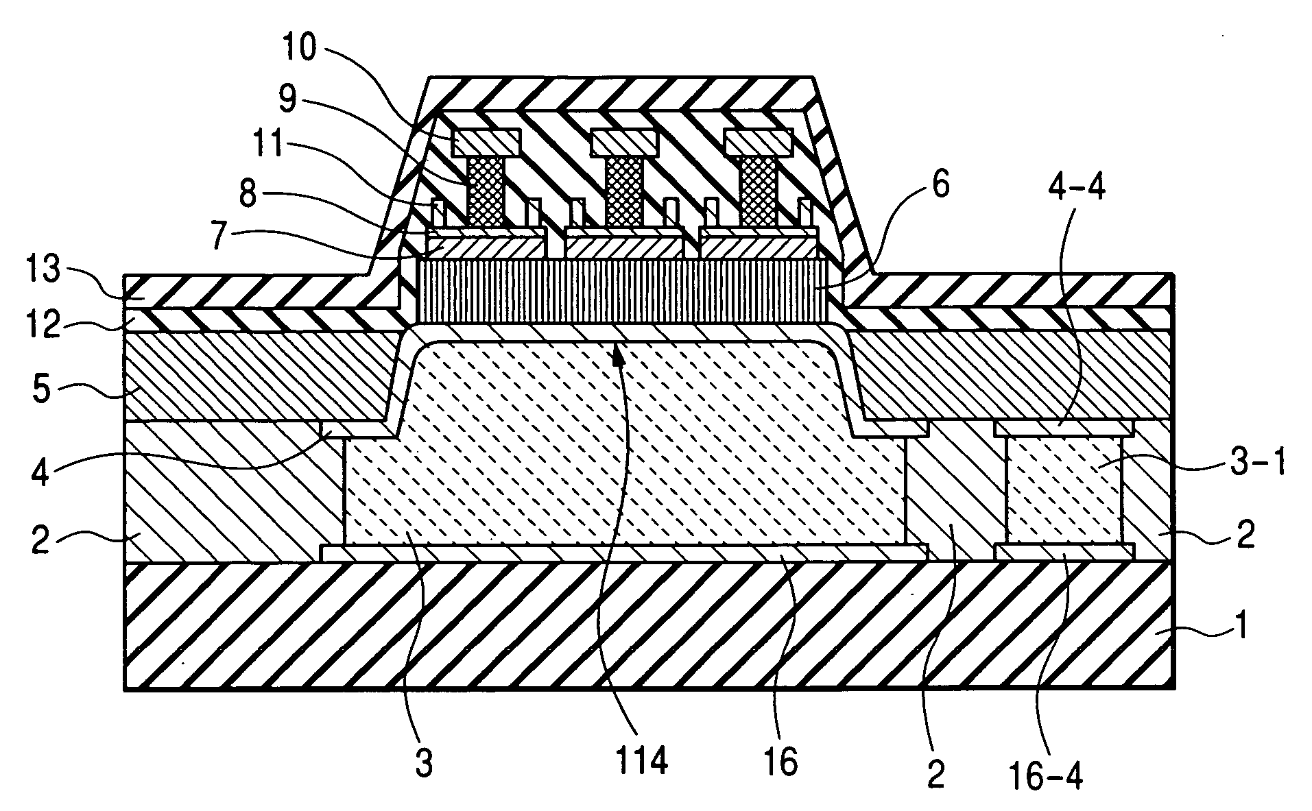
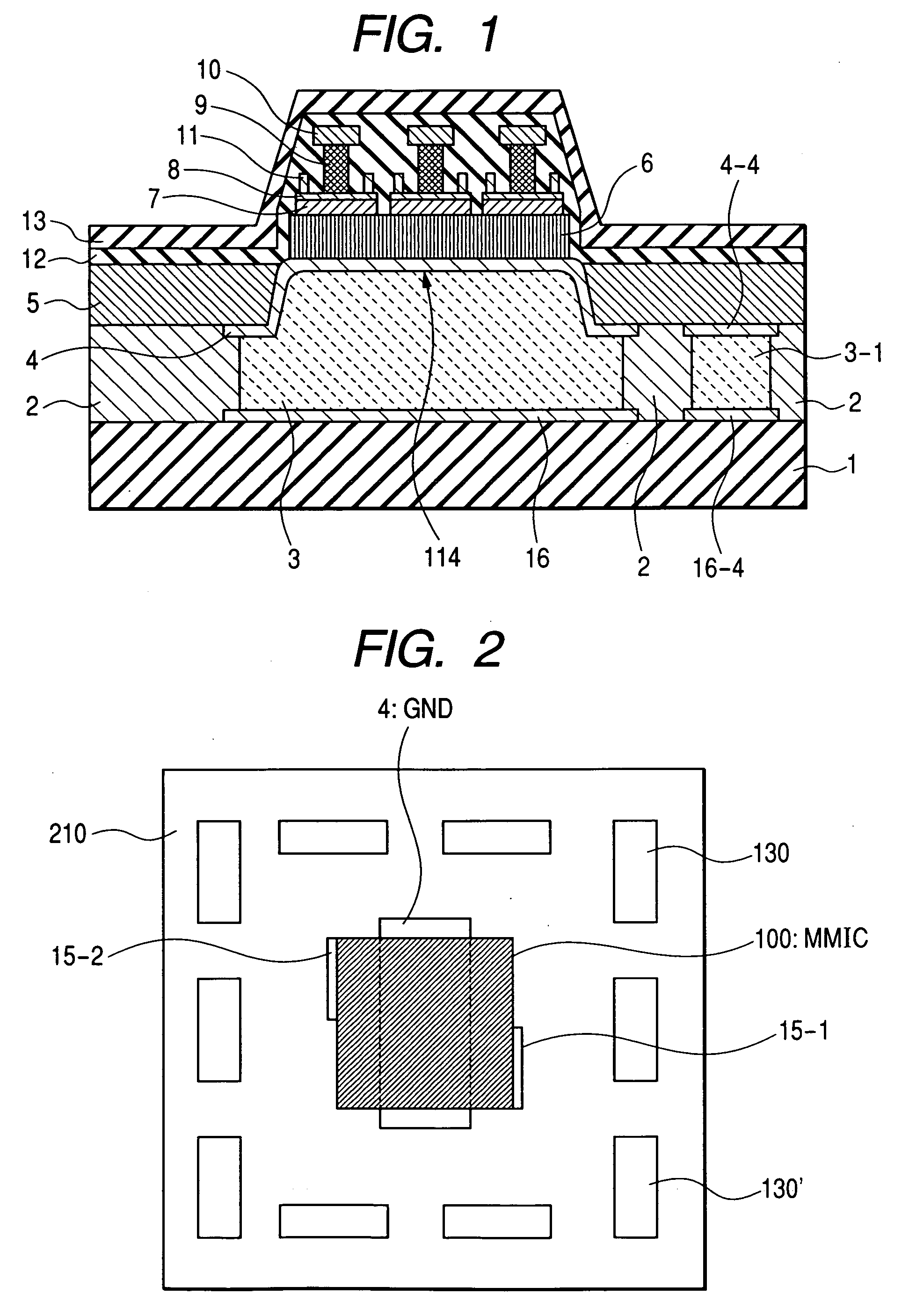
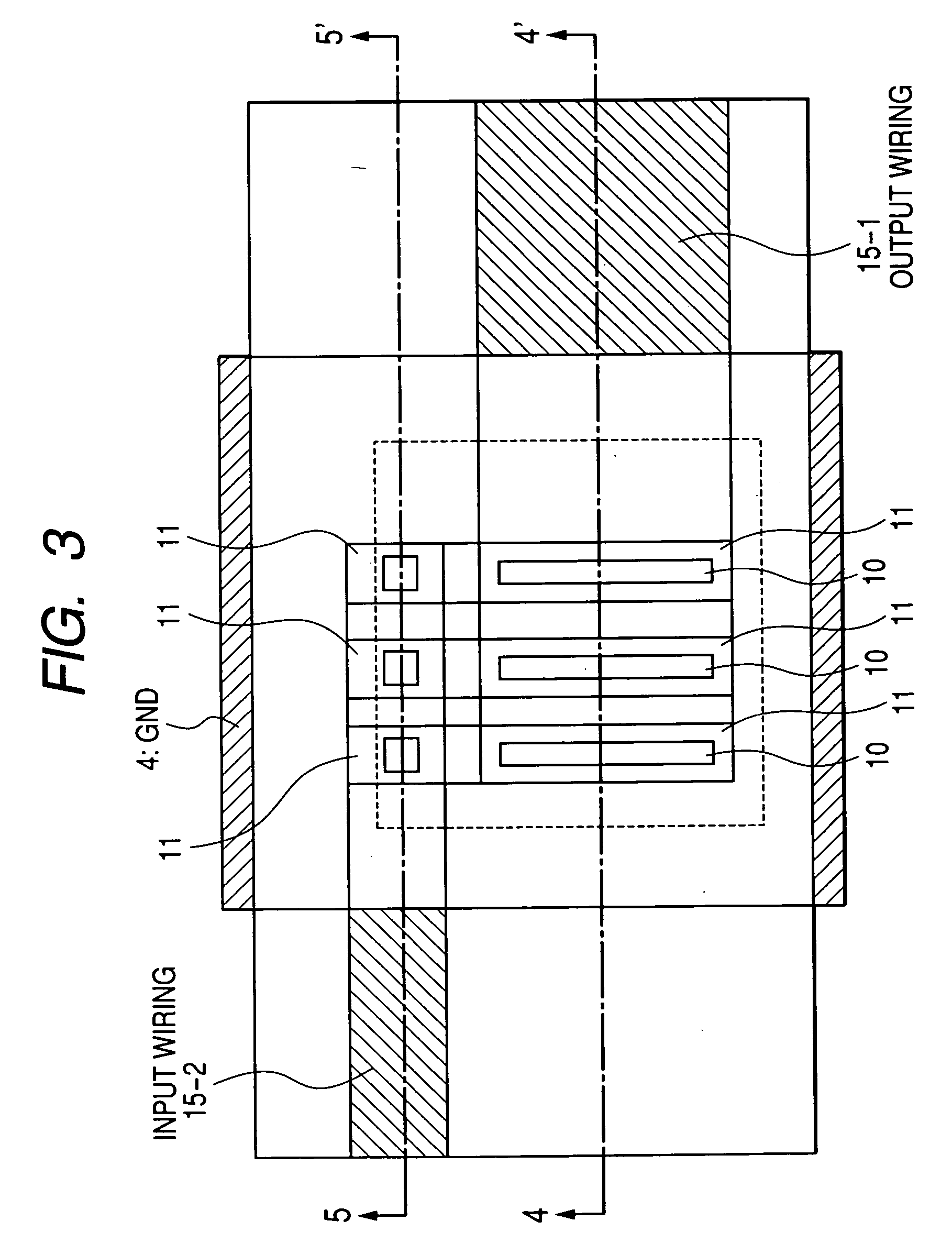
[0067] The present example is a power amplifier module. FIG. 2 is a general plan view of the present example. FIG. 3 is an enlarged top view of a MMIC (100) and its vicinity. FIGS. 4 and 5 show longitudinal cross-sectional views of this MMIC used in the present power amplifier module. These longitudinal cross-sectional views respectively correspond to lines 55′ and 44′ in FIG. 3FIG. 6 is a schematic cross-sectional view of the present power amplifier module embodiment. FIG. 6 schematically shows the mutual relations of individual members stacked in the module. Note that a collector up HBT is used in the present MMIC embodiment.
[0068] As indicated by the module layout of FIG. 2, the MMIC (100) is mounted on a module substrate 210 and other chip members 130 and 130′ which are, for example, passive components are located around it. Note that the other rectangles, shown around the MMIC (100) and chip members 130 and 130′ in FIG. 2, are also chip devices required in this module although...
embodiment 2
[0084] The following describes a typical method of manufacturing a semiconductor device. FIGS. 13 to 20 are cross sectional views of a device to explain how the semiconductor device is manufactured in accordance with the present invention. This example manufactures a high power multi-fingered HBT composed of basic HBTs which are connected in parallel.
[0085] Firstly, a highly doped n-type GaAs sub-emitter layer (Si concentration 5×1018 cm−3, thickness 0.8 μm) 6, a n-type InGaP emitter layer (InP molar ratio 0.5, Si concentration 5×1017 cm−3, thickness 0.2 μm) 7, a p-type GaAs base layer (C concentration 3×1019 cm−3, thickness 70 nm) 8 and a n-type InGaAs collector layer (Si doped, thickness 0.8 μm) 9 are grown on a semi-insulation GaAs substrate 5 by metalorganic vapor phase epitaxy. In the InGaAs collector layer, the InAs molar ratio varies from 0 to 0.5 and the Si concentration varies from 3×1016 cm−3 to 2×1019 cm−3.
[0086] Then, after a WSi layer (WSi: Si molar ratio 0.3, thickne...
embodiment 3
[0099] The following describes a power amplifier module embodiment which uses a different HBT-MMIC. The HBT-MMIC in this power amplifier module is made from an InP compound semiconductor, not a GaAs compound semiconductor used in Embodiment 1. Hereinafter, the HBT-MMIC which uses InP compound semiconductor material is simply denoted as “InPHBT-MMIC”.
[0100] Basically, the InPHBT-MMIC has the same structure as that of Embodiment 1, namely the structure shown in FIGS. 4 and 5. In terms of materials, the back side electrode 4 is a Ti (thickness 50 nm) / Au (10 im) layer, the semiconductor substrate 5 is a semi-insulation InP substrate, the sub-emitter layer 6 is a highly doped n-type InGaAs layer (InAs molar ratio 0.5, Si concentration 2×1019 cm−3, thickness 0.8 im), the emitter layer 7 is a n-type InAlAs (InAs molar ratio 0.5, Si concentration 3×1017 cm−3, thickness 0.2 im), the base layer 8 is a p-type InGaAs (InAs molar ratio 0.5, C concentration 3×1019 cm−3, thickness 70 nm) and the ...
PUM
 Abstract
Description
Claims
Application Information


