Semiconductor HBT MMIC device and semiconductor module

a technology of semiconductor modules and mmics, which is applied in the direction of semiconductor devices, semiconductor/solid-state device details, electrical apparatus, etc., can solve the problems of difficult to secure the mechanical strength of the mmic itself, difficulty in reliability, and differences between components and electrical members of the module substrate, and achieve satisfactory and mechanical strength. satisfactory, satisfactory in terms of mechanical strength, miniaturization and thermal stability

Inactive Publication Date: 2009-06-16
RENESAS ELECTRONICS CORP
View PDF10 Cites 3 Cited by
  • Summary
  • Abstract
  • Description
  • Claims
  • Application Information

AI Technical Summary

Benefits of technology

[0017]Openings may be filled until projections occur from the back surface of the semiconductor substrate. These projections make it easier to integrate other electrical members on the back side of the semiconductor substrate. The maximum height from the back side of the semiconductor substrate is dependent on the maximum allowable resist thickness.
[0031]According to the present invention, it is possible to provide a semiconductor device which is satisfactory in terms of mechanical strength, miniaturization and thermal stability. According to another aspect of the present invention, it is possible to provide a manufacturing method capable of manufacturing a semiconductor device which is satisfactory in terms of mechanical strength, miniaturization and thermal stability. According to yet another aspect of the present invention, it is possible to provide a semiconductor module which is satisfactory in terms of mechanical strength, miniaturization and thermal stability.

Problems solved by technology

This configuration has a structural problem that the conductor layers required to connect the components and electrical members to the module substrate differ in thickness namely due to the different thicknesses of the components and electrical members.
Accordingly, it is difficult to secure the mechanical strength of the MMIC itself.
This causes some difficulties in reliability.
These many electrical contact points are disadvantageous in terms of durability, too.
Prior art structures have a problem in terms of usability, too.
Therefore, it is not possible to form wiring lines, etc. on the back side of the semiconductor substrate.
In addition, if no bump is formed below the active component, that is, all bumps are formed on the back side of the semiconductor substrate only to connect components to the module substrate, thermal radiation from the active component in the MMIC to the back side of the semiconductor substrate may not be satisfactory, resulting in unstable operation of the active component.

Method used


Image

  • Semiconductor HBT MMIC device and semiconductor module
  • Semiconductor HBT MMIC device and semiconductor module
  • Semiconductor HBT MMIC device and semiconductor module

Examples


embodiment 1

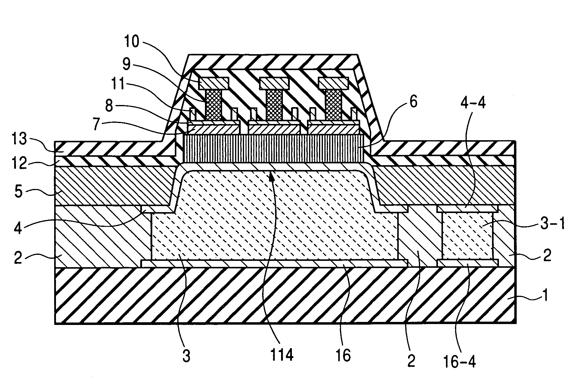
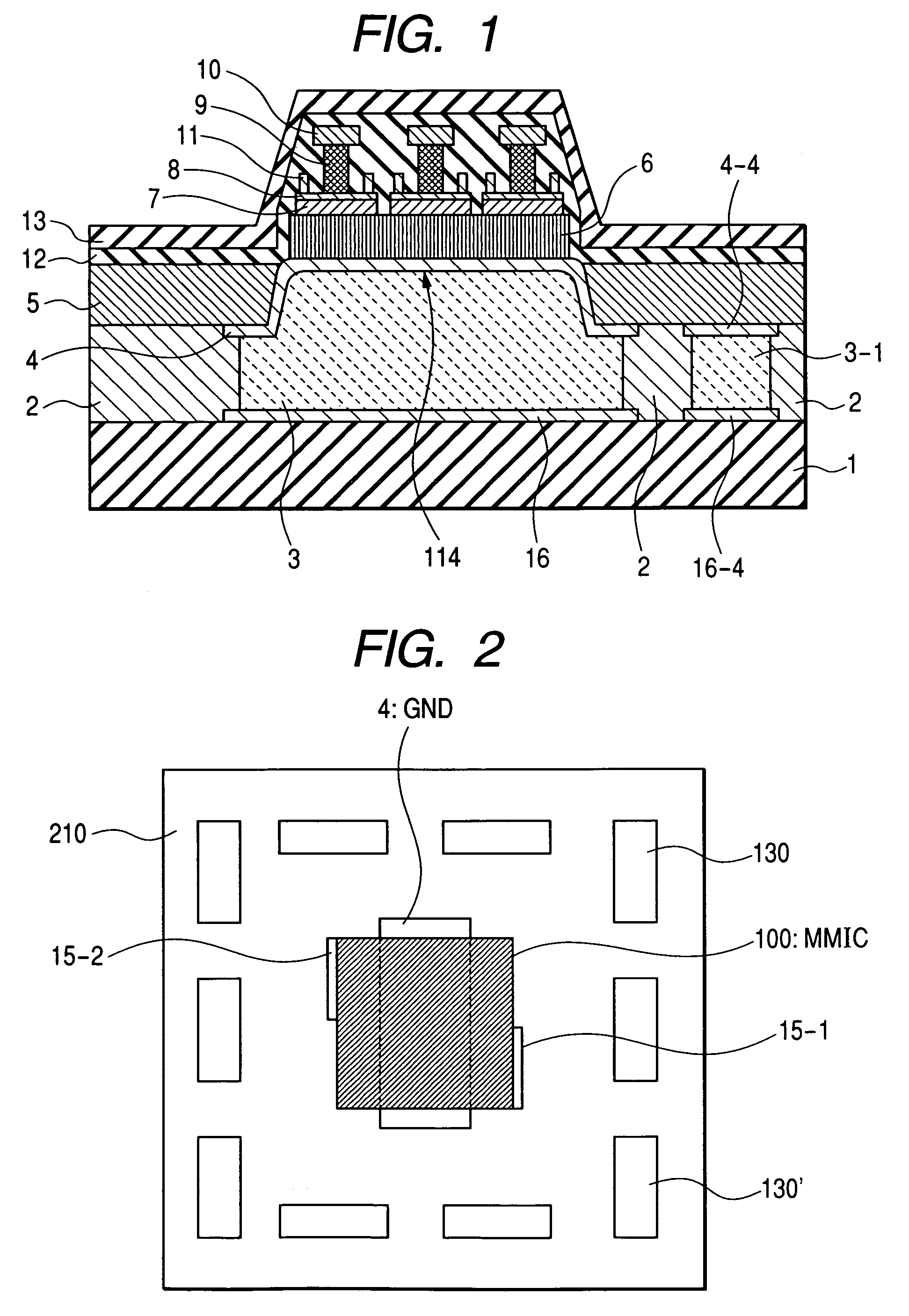
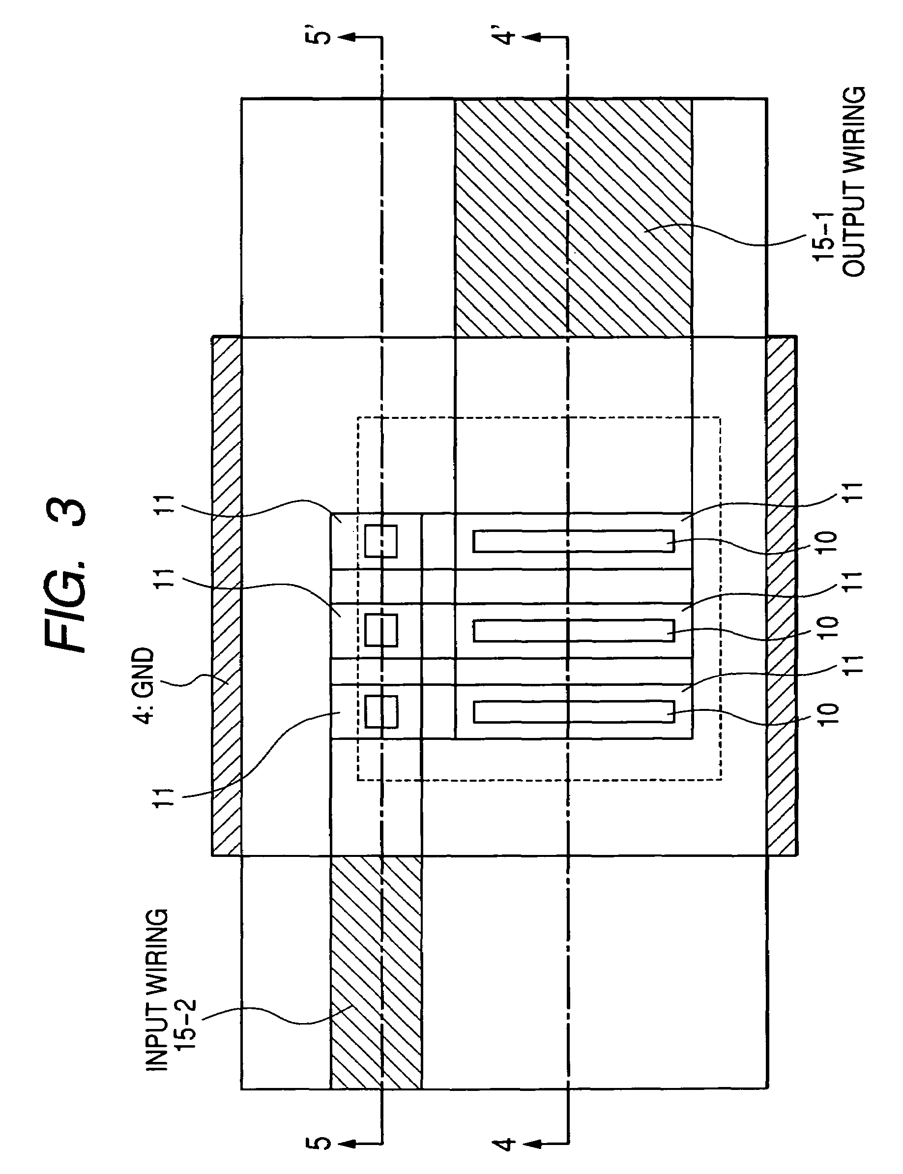
[0067]The present example is a power amplifier module. FIG. 2 is a general plan view of the present example. FIG. 3 is an enlarged top view of a MMIC (100) and its vicinity. FIGS. 4 and 5 show longitudinal cross-sectional views of this MMIC used in the present power amplifier module. These longitudinal cross-sectional views respectively correspond to lines 55′ and 44′ in FIG. 3FIG. 6 is a schematic cross-sectional view of the present power amplifier module embodiment. FIG. 6 schematically shows the mutual relations of individual members stacked in the module. Note that a collector up HBT is used in the present MMIC embodiment.

[0068]As indicated by the module layout of FIG. 2, the MMIC (100) is mounted on a module substrate 210 and other chip members 130 and 130′ which are, for example, passive components are located around it. Note that the other rectangles, shown around the MMIC (100) and chip members 130 and 130′ in FIG. 2, are also chip devices required in this module although th...

embodiment 2

[0084]The following describes a typical method of manufacturing a semiconductor device. FIGS. 13 to 20 are cross sectional views of a device to explain how the semiconductor device is manufactured in accordance with the present invention. This example manufactures a high power multi-fingered HBT composed of basic HBTs which are connected in parallel.

[0085]Firstly, a highly doped n-type GaAs sub-emitter layer (Si concentration 5×1018 cm−3, thickness 0.8 μm) 6, a n-type InGaP emitter layer (InP molar ratio 0.5, Si concentration 5×1017 cm−3, thickness 0.2 μm) 7, a p-type GaAs base layer (C concentration 3×1019 cm−3, thickness 70 nm) 8 and a n-type InGaAs collector layer (Si doped, thickness 0.8 μm) 9 are grown on a semi-insulation GaAs substrate 5 by metalorganic vapor phase epitaxy. In the InGaAs collector layer, the InAs molar ratio varies from 0 to 0.5 and the Si concentration varies from 3×1016 cm−3 to 2×1019 cm−3.

[0086]Then, after a WSi layer (WSi: Si molar ratio 0.3, thickness 0....

embodiment 3

[0099]The following describes a power amplifier module embodiment which uses a different HBT-MMIC. The HBT-MMIC in this power amplifier module is made from an InP compound semiconductor, not a GaAs compound semiconductor used in Embodiment 1. Hereinafter, the HBT-MMIC which uses InP compound semiconductor material is simply denoted as “InPHBT-MMIC”.

[0100]Basically, the InPHBT-MMIC has the same structure as that of Embodiment 1, namely the structure shown in FIGS. 4 and 5. In terms of materials, the back side electrode 4 is a Ti (thickness 50 nm) / Au (10 ìm) layer, the semiconductor substrate 5 is a semi-insulation InP substrate, the sub-emitter layer 6 is a highly doped n-type InGaAs layer (InAs molar ratio 0.5, Si concentration 2×1019 cm−3, thickness 0.8 im), the emitter layer 7 is a n-type InAlAs (InAs molar ratio 0.5, Si concentration 3×1017 cm−3, thickness 0.2 im), the base layer 8 is a p-type InGaAs (InAs molar ratio 0.5, C concentration 3×1019 cm−3, thickness 70 nm) and the col...


PUM


Abstract

The present invention provides a semiconductor device which comprises active components, passive components, wiring lines and electrodes and are satisfactory in terms of mechanical strength, miniaturization and thermal stability. In the semiconductor device, openings are formed just below active components. These openings are filled with conductor layers. Conductor layers are also formed where openings are not formed.

Description

CLAIM OF PRIORITY[0001]The present application claims priority from Japanese application JP 2004-301225 filed on Oct. 15, 2004, the content of which is hereby incorporated by reference into this application.BACKGROUND OF THE INVENTION[0002]1. Field of the Invention[0003]The present invention relates to a small-sized high reliability semiconductor device, a manufacturing method thereof and a semiconductor module which uses the same.[0004]2. Description of the Related Art[0005]Recently, along with rapidly growing demands for mobile communication apparatus, power amplifiers for them have become a target of energetic research and development activities. To meet the needs for smaller communication apparatus, monolithic microwave integrated circuits (MMICs), which are small semiconductor chips with built-in passive components, are incorporated in power amplifier modules. In these ICs, heterojunction bipolar transistors (HBTs) are mainly used since they allow high power densities and minia...

Claims


Application Information

Patent Timeline
Patent Type & Authority Patents(United States)
IPC IPC(8): H01L29/40
CPCH01L23/482H01L2924/01078H01L2924/01079H01L2924/09701H01L2924/16152H01L2924/19041H01L2924/1423H01L24/48H01L2224/48091H01L2224/48227H01L2924/1305H01L2924/12041H01L2924/30107H01L2924/00014H01L2924/00H01L2924/14H01L2224/45099H01L2224/45015H01L2924/207
Inventor TANAKA, KENICHIMATSUMOTO, HIDETOSHIOHBU, ISAOMOCHIZUKI, KAZUHIROTANOUE, TOMONORITAKUBO, CHISAKIUCHIYAMA, HIROYUKI
Owner RENESAS ELECTRONICS CORP
Why Eureka
Try Eureka