Structure and method for adjusting integrated circuit resistor value

a technology of resistor value and integrated circuit, which is applied in the field of resistors, can solve the problems of time-consuming and expensive processes employed to design and fabricate each mask, limited range of available resistances, and small number of spare resistors of different resistance values that can be readily and practically fabricated in the integrated circui

Active Publication Date: 2006-04-27
BELL SEMICON LLC
View PDF10 Cites 11 Cited by
  • Summary
  • Abstract
  • Description
  • Claims
  • Application Information

AI Technical Summary

Benefits of technology

[0015] A first embodiment of the invention comprises a resistor comprising a bar of resistive material, a dielectric material layer disposed over the bar, a plurality of contacts disposed in the dielectric material layer and having a lower end in electrical contact with the bar; and a first and a second interconnect structure disposed over the dielectric material layer, each in electrical contact with an upper end of a first and a second contact of the plurality of contacts, such that an electrical current path is formed from the first interconnect structure, through the first contact, a current-carrying region of the bar and the second contact to the second interconnect structure, and wherein the first and the second contacts are disposed relative to the plurality of contacts to provide a predetermined resistance through the current-carrying region of the bar.
[0016] Another embodiment of the present invention comprises a method for form

Problems solved by technology

As is known in the art, the processes employed to design and fabricate each mask are time intensive and expensive.
Disadvantageously, a range of available resistances may be limited as in practice the number of spare resistors of different resistance values that can be readily and practically fabricated in the integrated circuit is relatively small.
Also, it may be difficult to modify the interconnect structures to accommodate a different resistor, and further the modification may involve changing in

Method used


Image

  • Structure and method for adjusting integrated circuit resistor value
  • Structure and method for adjusting integrated circuit resistor value
  • Structure and method for adjusting integrated circuit resistor value

Examples


Embodiment Construction

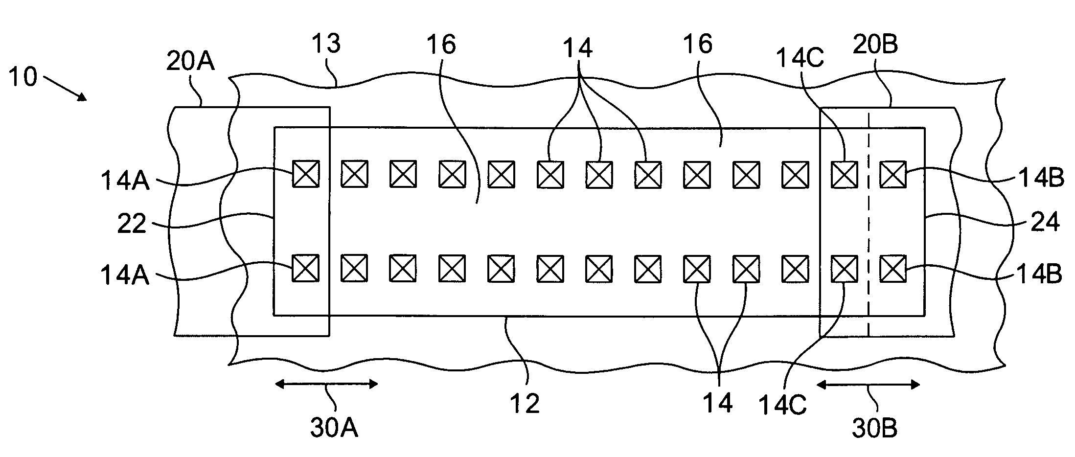
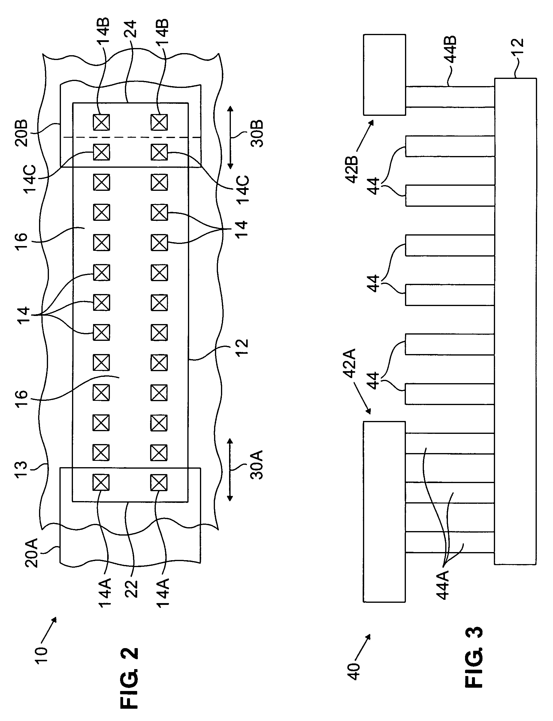
[0023] Before describing in detail the particular structure and method for adjusting resistor values in an integrated circuit, it should be observed that the present invention resides primarily in a novel and non-obvious combination of elements and process steps. So as not to obscure the disclosure with details that will be readily apparent to those skilled in the art, certain conventional elements and steps have been presented with lesser detail, while the drawings and the specification describe in greater detail other elements and steps pertinent to understanding the invention.

[0024] In conjunction with the description of the present invention, the term “window-1” layer refers to an interconnect structure formed in a first dielectric layer and comprising conductive vias or plugs in electrical contact with resistive material and other elements formed in the semiconductor substrate. “Metal-1” refers to an interconnect structure layer comprising metal interconnect lines overlying th...


PUM


Abstract

A resistor formed on a material layer of a semiconductor integrated circuit and a method for forming the resistor. The resistor comprises a region of resistive material with a plurality of conductive contacts or plugs in electrical contact with and extending away from the resistive material. A first and a second interconnect line are formed overlying the plugs and in conductive contact with one or more of the plurality of plugs, such that a portion of the resistive material between the first and the second interconnect lines provides a desired resistance. According to a method of the present invention, the plurality of conductive contacts are formed using a first photolithographic mask and the first and the second interconnect lines are formed using a second photolithographic mask. The desired resistance is changed by modifying the first or the second mask such that one or more dimensions of a region of the resistive material between the first and the second interconnect lines is altered.

Description

FIELD OF THE INVENTION [0001] This invention relates generally to resistors formed in integrated circuits and specifically to an apparatus and method for adjusting a value of the resistor. BACKGROUND OF THE INVENTION [0002] Integrated circuits (also referred to as chips or die) typically comprise a silicon substrate and active semiconductor devices, such as transistors and diodes, and passive components, such as capacitors and resistors, formed from doped regions within the substrate. Passive components can also be formed in material layers overlying the substrate, e.g., polysilicon resistors formed in a polysilicon layer overlying the silicon substrate. [0003] Interconnect structures, also formed in layers overlying the semiconductor substrate, electrically connect the doped regions and the passive components to form a functional integrated circuit. The interconnect structures comprise a plurality of stacked substantially horizontal conductive layers comprising conductive metal int...

Claims


Application Information

Patent Timeline
IPC IPC(8): H01C1/012H01L21/02
CPCH01L23/5228H01L28/20H01L2924/0002H01L2924/00H01C7/006H01L23/647H05K1/167
Inventor KERR, DANIEL CHARLESKEY, ROGER W.ALBERS, BRADLEY J.RUSSELL, WILLIAM A.CHEN, ALAN SANGONE
Owner BELL SEMICON LLC
Why Eureka
Try Eureka