Supercharge Your Innovation With Domain-Expert AI Agents!

Semiconductor device having metal silicide and method of making the same

a technology of metal silicide and semiconductor devices, which is applied in the direction of semiconductor devices, electrical devices, transistors, etc., can solve the problems of agglomeration problems, narrow device line widths, and shallow junctions, and achieve the effect of reducing sheet resistance and improving thermal stability

Inactive Publication Date: 2006-05-04
UNITED MICROELECTRONICS CORP
View PDF7 Cites 9 Cited by
  • Summary
  • Abstract
  • Description
  • Claims
  • Application Information

AI Technical Summary

Benefits of technology

The present invention provides semiconductor devices with salicided polysilicon layers that have significantly reduced sheet resistance and improved thermal stability. Additionally, the invention provides a MOSFET device with a salicided polysilicon gate and a method for eliminating agglomeration during fabrication. The MOS transistor device includes a polysilicon gate with dielectric spacers and a first metal silicide layer that is formed from an upper exposed portion of the polysilicon gate and is at the top of the gate. The invention also includes a diffusion region that forms a second metal silicide layer. The first metal silicide layer has a greater vertical height than the second metal silicide layer. These technical effects improve the performance and reliability of semiconductor devices.

Problems solved by technology

However, the device line widths become narrower and the junctions become shallower as the transistor devices become smaller.
Further, a so-called agglomeration problem arises when a metal layer such as cobalt reacts at high temperatures with a polysilicon gate having a gate length that is approximately below 50 nm.
The agglomeration problem adversely affects the thermal stability of the salicide and therefore the performance of the gate when operating the transistor device.

Method used


Image

  • Semiconductor device having metal silicide and method of making the same
  • Semiconductor device having metal silicide and method of making the same
  • Semiconductor device having metal silicide and method of making the same

Examples


Embodiment Construction

[0015] The present invention will now be described with reference to the attached figures. The present invention is understood to be of particular advantage when employed for forming the metal silicide layers of MOS transistor devices. For this reason, examples will be given in the following in which corresponding embodiments of the present invention are utilized for forming the metal silicide layers of a MOS transistor.

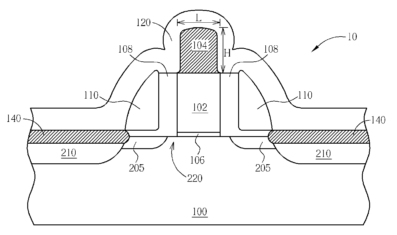
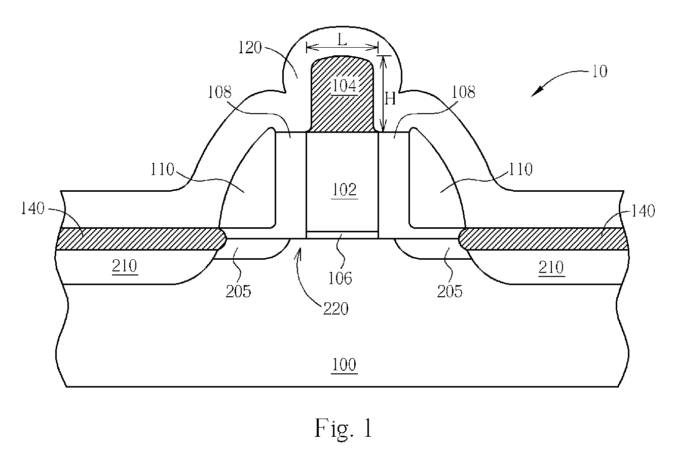
[0016]FIG. 1 is a schematic cross-sectional diagram demonstrating a MOS transistor 10 having an improved metal silicide layer 104 formed at top of the polysilicon gate 102 of the MOS transistor in accordance with the present invention. As shown in FIG. 1, the MOS transistor 10 is fabricated on a semiconductor substrate 100. The semiconductor substrate 100 can be either P- or N-type substrate, depending on the type of MOS transistor 10. In another embodiment, the semiconductor substrate 100 may be a silicon-on-insulator (SOI) substrate. It is to be understood that th...


PUM


Abstract

A MOS transistor device includes a polysilicon gate with opposing sidewalls over an active area of a semiconductor substrate. The polysilicon gate has a gate length “L”. Dielectric spacers are disposed at a lower portion of the opposing sidewalls of the polysilicon gate. A metal silicide layer is situated approximately a vertical height “H” above a top surface of the dielectric spacers. The metal silicide layer is formed from an upper exposed portion of the polysilicon gate. Most importantly, the vertical height “H” is greater than the gate length “L” (H>L rule). A diffusion region is implanted into the semiconductor substrate and is adjacent to the polysilicon gate.

Description

BACKGROUND OF INVENTION [0001] 1. Field of the Invention [0002] The present invention relates to the field of fabrication of integrated circuits, and, more particularly, to a semiconductor device with metal silicide portions formed therein. The formed metal silicide portions have improved thermal stability. A method for making such semiconductor device is also proposed, which can effectively solve the agglomeration problem. [0003] 2. Description of the Prior Art [0004] Field effect transistors represent the most frequently used circuit elements in modern integrated circuits. Typically, a huge number of field effect transistors is simultaneously formed on a substrate and are connected to establish the required functionality of the circuit. Generally, a field effect transistor comprises two highly doped drain and source regions that are embedded in a lightly and inversely doped silicon well region. The drain and the source regions are spaced apart with a channel region interposed, whe...

Claims


Application Information

Patent Timeline
Patent Type & Authority Applications(United States)
IPC IPC(8): H01L29/94
CPCH01L21/28052H01L21/28114H01L21/28123H01L29/665H01L29/6653H01L29/6656H01L29/6659H01L29/7833
Inventor LI, NIEN-CHUNG
Owner UNITED MICROELECTRONICS CORP
Features
  • R&D
  • Intellectual Property
  • Life Sciences
  • Materials
  • Tech Scout
  • Unparalleled Data Quality
  • Higher Quality Content
  • 60% Fewer Hallucinations
Learn More