Luminescence display panel

a technology of luminescence display panel and display panel, which is applied in the direction of discharge tube luminescence screen, static indicating device, instruments, etc., can solve the problems of difficult restraint of heat generation and deterioration of organic luminescence part, and achieve attractive visual effect, good image quality, and attractive

Inactive Publication Date: 2006-05-04
DAI NIPPON PRINTING CO LTD
View PDF6 Cites 15 Cited by
  • Summary
  • Abstract
  • Description
  • Claims
  • Application Information

AI Technical Summary

Benefits of technology

[0028] As described above, the present invention makes it possible to display a pattern such as a character, figure, sign, design, or static image, of a good image quality, by a combination of a luminescence region and non-luminescence region. Thus, the present invention can provide a luminescen

Problems solved by technology

When a high voltage is applied to the transparent electrode, there is concern that the heat generated by the flowing electricity may cause a deterioration in the organic luminescence part, a deformation in the transparent resin film serving as the substrate, or a burning of the

Method used


Image

  • Luminescence display panel
  • Luminescence display panel
  • Luminescence display panel

Examples


first embodiment

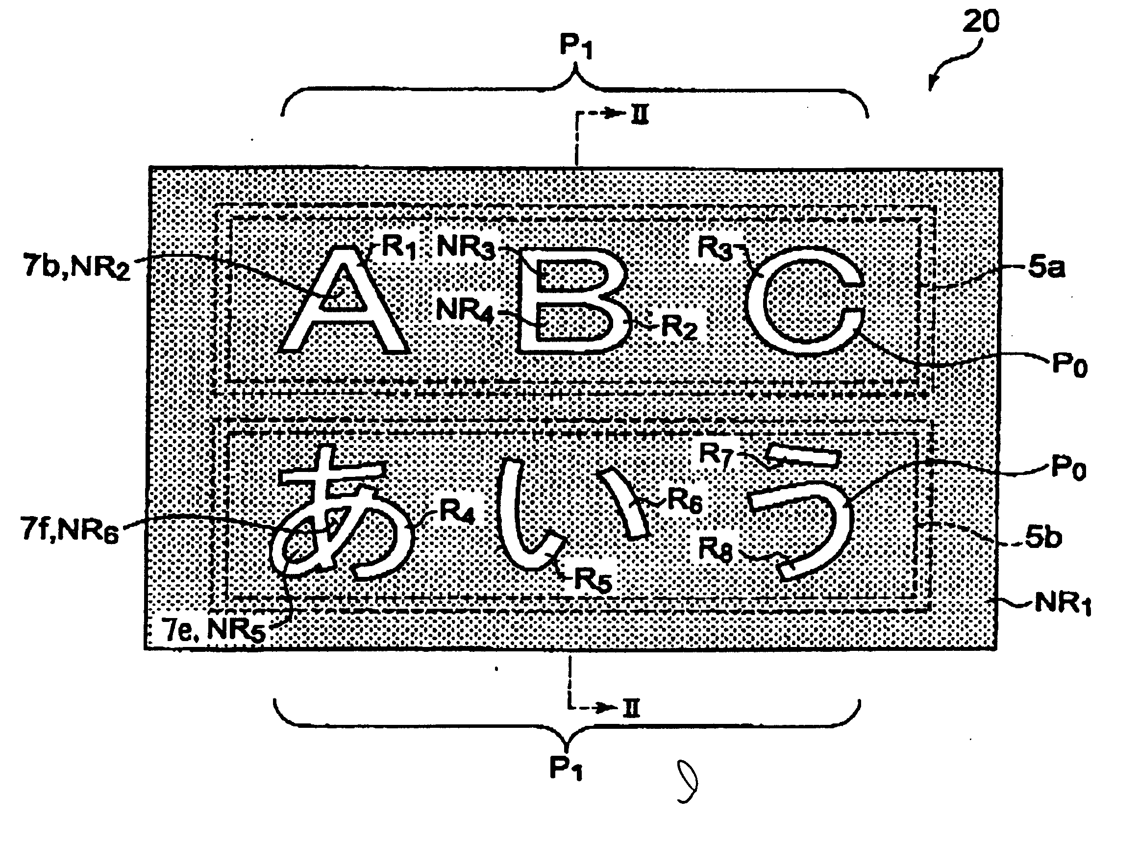
[0035]FIG. 1 is a schematic front view of a display surface of an example of a luminescence display panel according to the present invention.

[0036] As described above, a luminescence display panel according to the present invention displays a predetermined pattern (a character, figure, sign, design, static image, and so on) formed by a luminescence region and a non-luminescence region. As shown in FIG. 1, a luminescence display panel 20 displays thereon a character line of “ABC” in an upper half part and a character lie of “” (Japanese) in a lower half part, by a combination of eight luminescence regions R1 to R8 and six non-luminescence regions NR1 to NR6.

[0037] In FIG. 1, the predetermined pattern of “ABC”“” are shown. A character line (pattern line) P1, i.e., “ABC” is constituted by three characters (pattern elements) P0, i.e., “A”, “B”, and “C”.

[0038] In FIG. 1, the respective non-luminescence regions NR1 to NR6 are smudged in order to facilitate a differentiation from the lu...

second embodiment

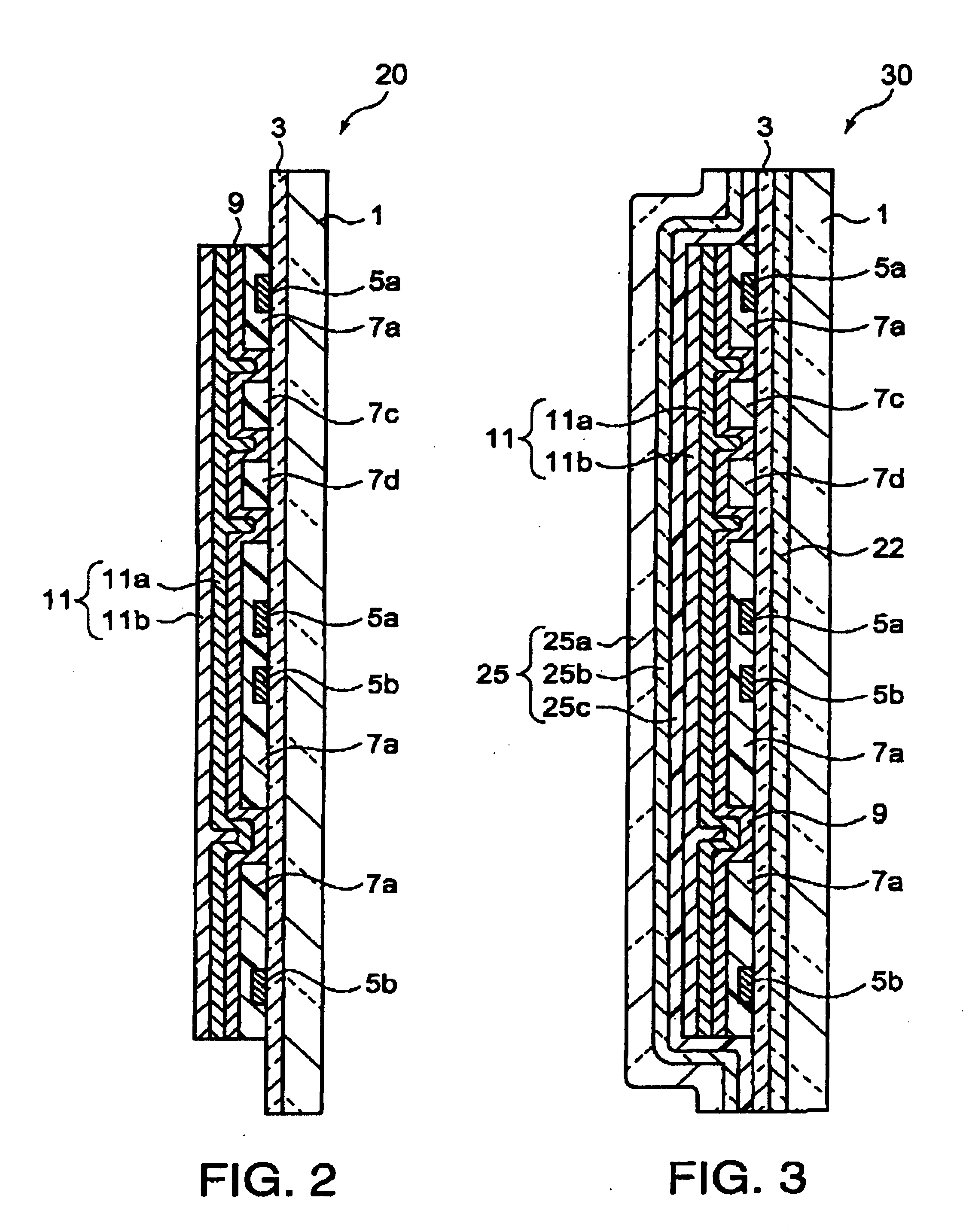
[0063] Since properties of an organic luminescent material used in an organic EL device are deteriorated by oxygen and moisture, the organic EL device is generally subjected to a sealing treatment for preventing an invasion of oxygen and moisture into an organic luminescence part. A luminescence display panel according to the present invention is preferably subjected to the sealing treatment.

[0064]FIG. 3 is a sectional view schematically showing an example of a luminescence display panel according to the present invention, which has been subjected to the sealing treatment. A luminescence display panel 30 shown in FIG. 3 has a constitution in which: a gas barrier layer 22 is disposed on a transparent substrate 1, which corresponds to the transparent substrate 1 of the luminescence display panel 20 shown in FIGS. 1 and 2; and a sealing layer 25 is disposed on a rear electrode 11. Except for the gas barrier layer 22 and the sealing layer 25, the constitution of the luminescence displa...

example 1

[0084] At first, a laminated resin film was prepared in which an ITO film having a film-thickness of 0.1 μm was formed on one surface of a polyether sulfone film having a film-thickness of 100 μm. In the laminated rein film, the polyether sulfone film corresponds to the “flexible transparent substrate” and the ITO film corresponds to the “transparent electrode” in the present invention.

[0085] Then, silver (Ag) was deposited on the transparent electrode by a vacuum deposition method with a use of a deposition mask of a predetermined shape, so that two auxiliary electrodes each having the same shape as that of the auxiliary electrode 5a or 5b of the luminescence display panel 20 shown in FIG. 1 were formed. The two auxiliary electrodes were arranged on the same positions as those of the auxiliary electrodes 5a and 5b in the luminescence display panel 20 shown in FIG. 1. Each of the auxiliary electrodes has a thickness of 0.2 μm, and a line-width of 1 mm.

[0086] Next, the transparent ...


PUM


Abstract

A luminescence display panel 20 includes: a flexible transparent substrate 1; a transparent electrode 3 formed on the transparent substrate 1, over a luminescence region and a non-luminescence region; and auxiliary electrodes 5a and 5b formed on the transparent electrode 3, over the non-luminescence region. Electric insulation layers 7a, 7c, and 7d are formed over the non-luminescence region of the transparent electrode 3, so as to cover the auxiliary electrodes 5a and 5b. An organic luminescence part 9 is formed on the transparent electrode, at least over the luminescence region. A rear electrode 11 is formed on the organic luminescence part 9.

Description

BACKGROUND OF THE INVENTION [0001] 1. Field of the Invention [0002] The present invention relates to a luminescence display panel for displaying a pattern such as a character, figure, sign, design, or static image, by combining a luminescence region and non-luminescence region. More particularly, it pertains to a luminescence display panel which can be used as an electric decorative illumination panel or the like. [0003] 2. Background Art [0004] Recently, an organic electroluminescence device (hereinafter abbreviated as “organic EL device”) known as a kind of the electroluminescence device has been put into practical use as a picture element for a flat panel display of high flexibility, or as a paper-like surface light source. As disclosed in Japanese Patent Laid-Open Publication No. 2004-111158 (see, claims, sections [0006] to [0008], and FIGS. 4 and 5), a paper-like luminescence display panel has been developed. In this luminescence display panel, a non-luminescence region of a pr...

Claims


Application Information

Patent Timeline
IPC IPC(8): H01L51/00H01L27/32H01L51/52
CPCH01L27/3239H01L27/3283H01L51/5212H01L2251/5338H10K59/221H10K59/173H10K50/814H10K2102/311G09G3/12H05B33/04H10K50/805H10K50/86
Inventor SHIROGANE, HIROYUKIHANDA, SHINICHIKUBA, KENICHIKOBAYASHI, MASARU
Owner DAI NIPPON PRINTING CO LTD
Why Eureka
Try Eureka