Semiconductor memory chip, semiconductor memory module and method for transmitting write data to semiconductor memory chips

a semiconductor memory chip and write data technology, applied in the direction of digital transmission, error prevention, instruments, etc., can solve the problems of increasing the cost of such a device, not having a possibility for error detection or correction, and the dimm memory module of desktop personal computers that is not usually used for dimming, so as to achieve simple and cost-effective error correction

Inactive Publication Date: 2006-05-04
INFINEON TECH AG
View PDF10 Cites 4 Cited by
  • Summary
  • Abstract
  • Description
  • Claims
  • Application Information

AI Technical Summary

Benefits of technology

[0008] In view of the above, it is an object of the invention, in the case of a semiconductor memory chip equipped with an interface circuit of this type and also in the case of a semico

Problems solved by technology

However, customary DIMM memory modules for desktop personal computers do not usually have a possibility for error detection or correction.
An added fu

Method used


Image

  • Semiconductor memory chip, semiconductor memory module and method for transmitting write data to semiconductor memory chips
  • Semiconductor memory chip, semiconductor memory module and method for transmitting write data to semiconductor memory chips
  • Semiconductor memory chip, semiconductor memory module and method for transmitting write data to semiconductor memory chips

Examples


Embodiment Construction

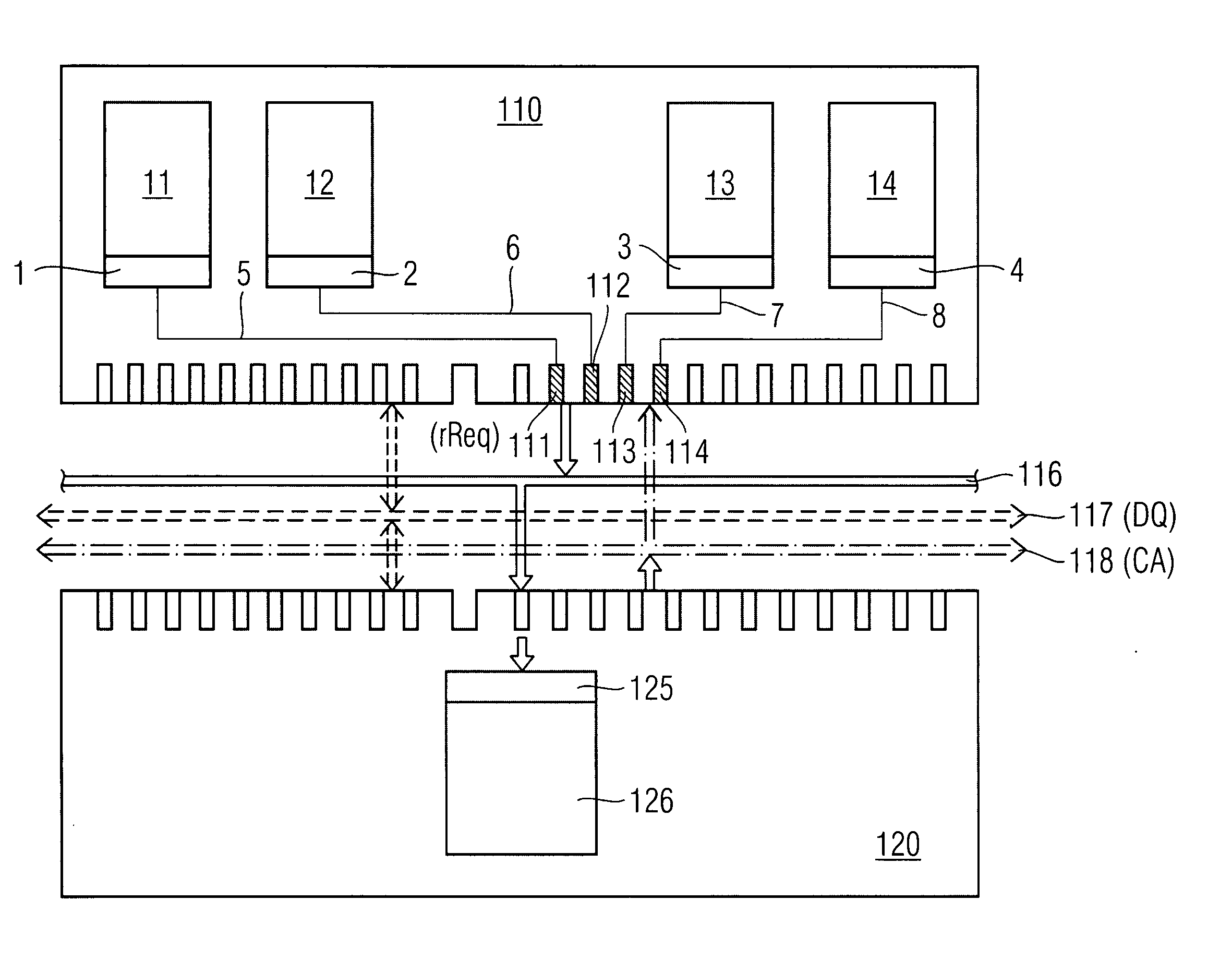
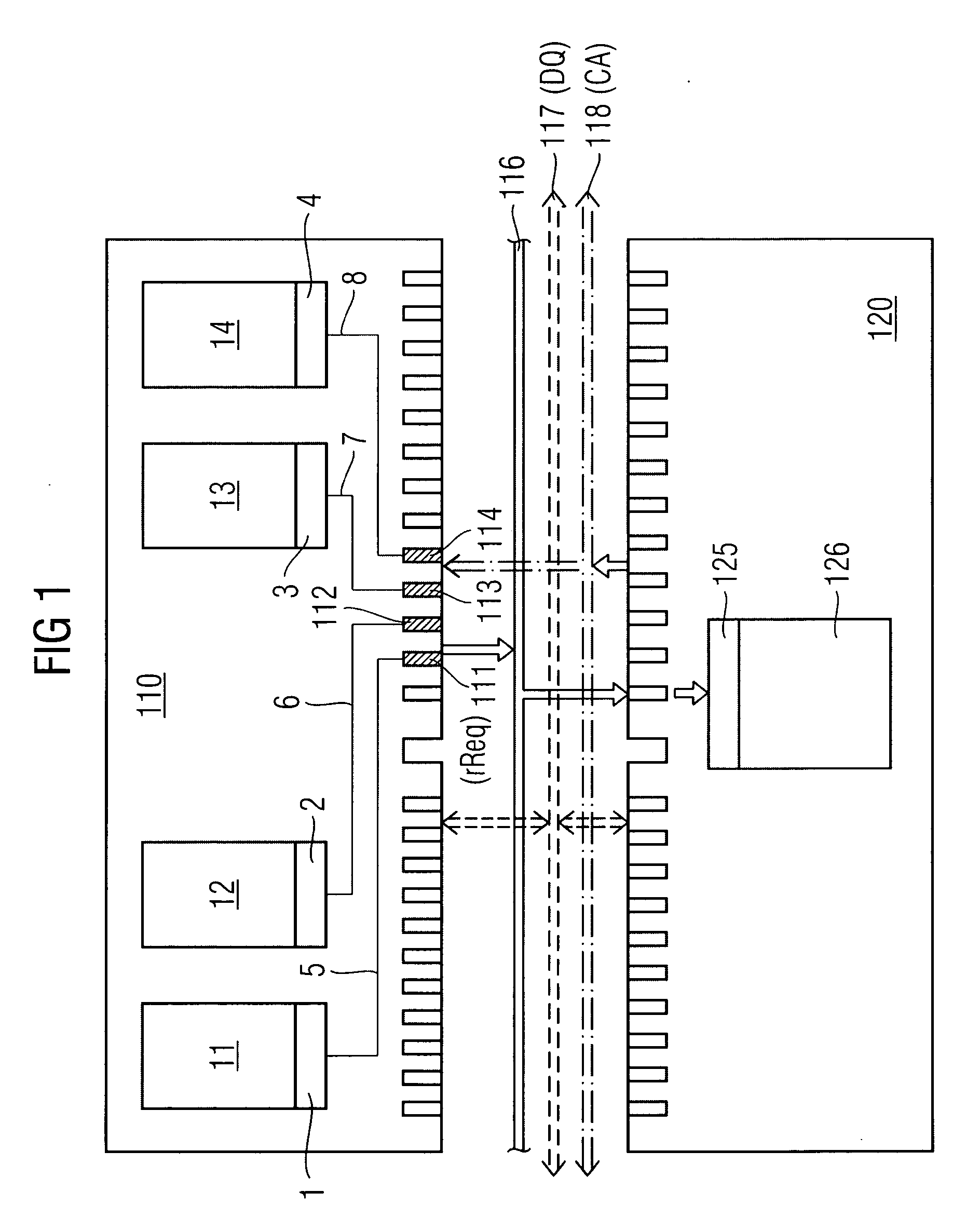
[0022] A common feature of each of the semiconductor memory modules 110, 210, 310 and 410 according to the invention that are illustrated schematically in FIGS. 1 to 4 is that they are equipped with a plurality (e.g. four) of semi-conductor memory chips 11 to 14 each including an interface circuit 1-4, which receive a write datum sent via a data bus (DQ bus) 117 from a memory controller 120, 220, 320 in response to a command and address signal transmitted via a CA bus 118, and are configured to detect a transmission error in the respectively received write datum (it should be noted that a DQ bus 117 and a CA bus 118 are shown only in FIG. 1 and are omitted in FIGS. 2 to 4 for a simplified illustration).

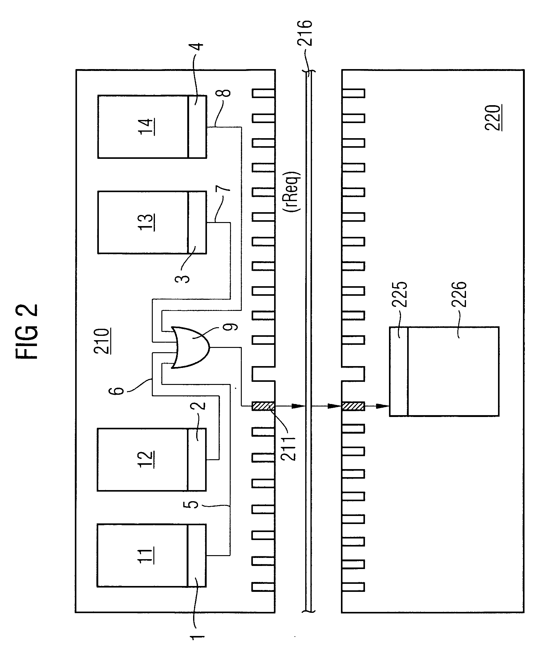
[0023] According to the invention, each interface circuit 1-4, if it has detected a transmission error in the write data, is configured to output, via a request signal path 5-8 (which are separate from the DQ bus) in FIGS. 1 and 2, 311-314 in FIG. 3, and 401, 411, 402, 412, 403, 413,...


PUM


Abstract

A semiconductor memory module includes a plurality of semiconductor memory chips. Each semiconductor memory chip includes an interface circuit that is configured to detect a transmission error in a write datum and is further configured to output, via a separate signal path, a repeat request signal for the repeated transmission of the write datum detected as erroneous. This repeat request signal can be transmitted either as a single-bit signal or as a multibit signal (e.g., serially as an individual signal line to a superordinate memory controller).

Description

CROSS REFERENCE TO RELATED APPLICATIONS [0001] This application claims priority under 35 USC § 119 to German Application No. DE 10 2004 052 612.5, filed on Oct. 29, 2004, and titled “Semicondcutor Memory Chip, Semiconductor Memory Module and Method for Transmitting Write Data to Semiconductor Memory Chips,” the entire contents of which are hereby incorporated by reference. FIELD OF THE INVENTION [0002] The invention relates to a semiconductor memory chip including an interface circuit which is set up at least for receiving write data and also for detecting a transmission error in the received write data, a semiconductor memory module equipped with a plurality of semiconductor memory chips of this type, and a method for transmitting write data to at least one semiconductor memory chip of this type. BACKGROUND [0003] At the increasing data transmission speeds of future DRAM generations, the data signals need to be transmitted differentially, which can increase the error protection in ...

Claims


Application Information

Patent Timeline
IPC IPC(8): H04L1/18G08C25/02
CPCG06F11/1044G11C5/063G11C7/10G11C11/4093
Inventor RUCKERBAUER, HERMANNSAVIGNAC, DONINIQUEGREGORIUS, PETERSICHERT, CHRISTIANWALLNER, PAUL
Owner INFINEON TECH AG
Why Eureka
Try Eureka