Temperature measurement and heat-treating methods

a technology of temperature measurement and heat treatment, applied in the direction of optical radiation measurement, chemical vapor deposition coating, vacuum evaporation coating, etc., can solve the problems of significant temperature measurement error, inability to accurately directly measure, and inability to produce sufficiently shallow junctions to meet the requirements of conventional techniques

Active Publication Date: 2006-05-11
MATTSON TECHNOLOGY +1
View PDF99 Cites 44 Cited by
  • Summary
  • Abstract
  • Description
  • Claims
  • Application Information

AI Technical Summary

Benefits of technology

[0028] Certain specific embodiments of the present invention may provide ways to obtain accurate temperature measurements of the device side of the wafer during the course of the flash. These accurate temperature measurements may then be used for feedback-control of the power of the flash, if desired, to ensure consistency of the flash and the resulting annealing process from wafer to wafer. Alternatively, even if such temperature measurements are not used for feedback-control, they may be useful in identifying system “drift”, or inconsistencies developing between successive executions of thermal processes that are supposed to be identical. Identification of such inconsistencies at an early stage may allow the users of the system to correct the inconsistencies as they are developing, rather than processing a large number of wafers only to discover that poor reproducibility control of the thermal processing cycle has led to detrimental performance differences from wafer to wafer.

Problems solved by technology

For example, where the workpiece is a semiconductor wafer, although the temperature of a substrate side of the wafer may often be measured directly, it is not possible to accurately directly measure the temperature of the device side of the wafer, as the non-uniform patterning of devices on the device side gives rise to significant variations in both scattering and emissivity from location to location across the device side, resulting in significant temperature measurement errors.
However, these conventional techniques cannot produce sufficiently shallow junctions to comply with current and upcoming industry requirements.
However, as noted, conventional methods are not adequate to accurately measure the temperature of the device side for this purpose.

Method used


Image

  • Temperature measurement and heat-treating methods
  • Temperature measurement and heat-treating methods
  • Temperature measurement and heat-treating methods

Examples


first embodiment

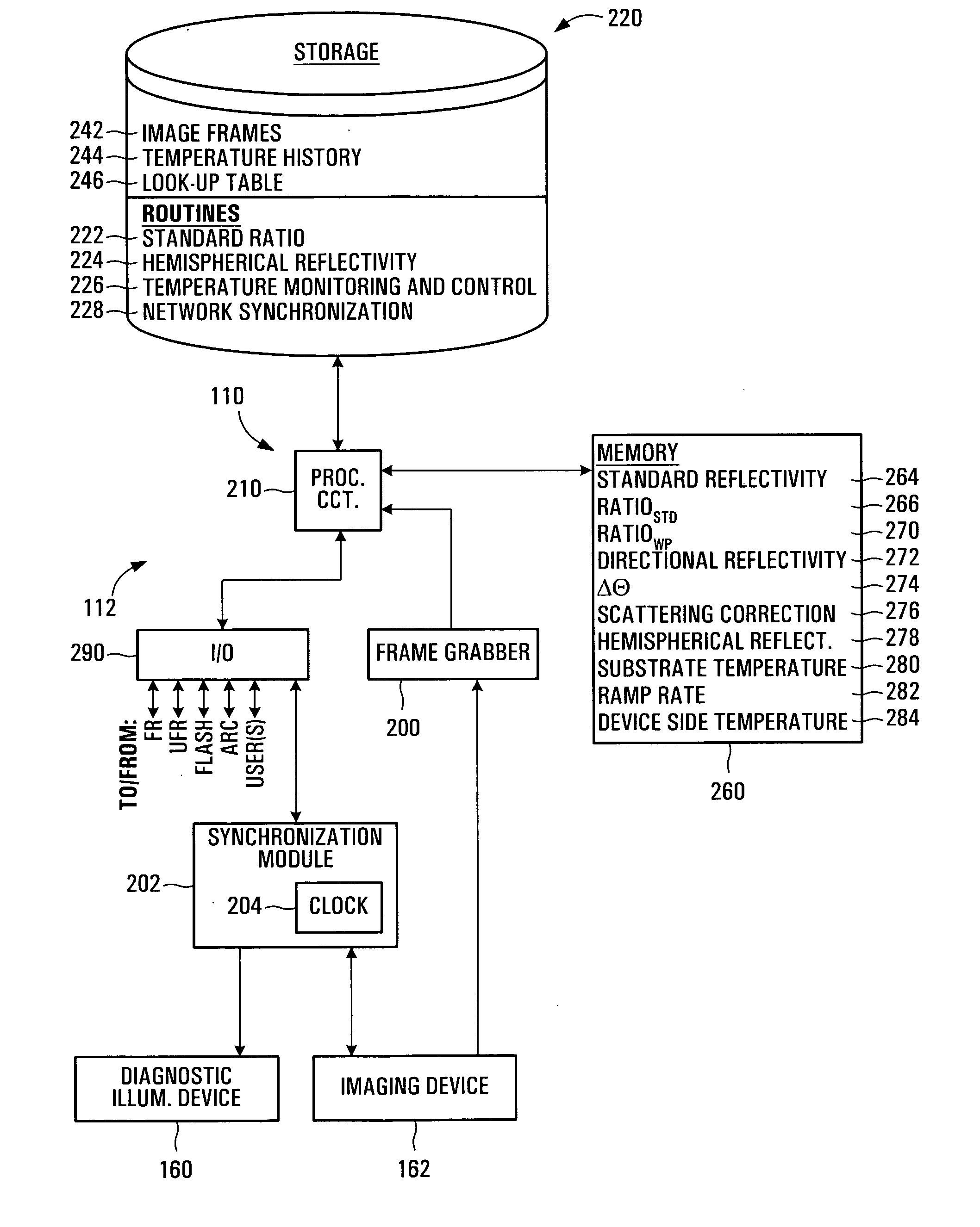
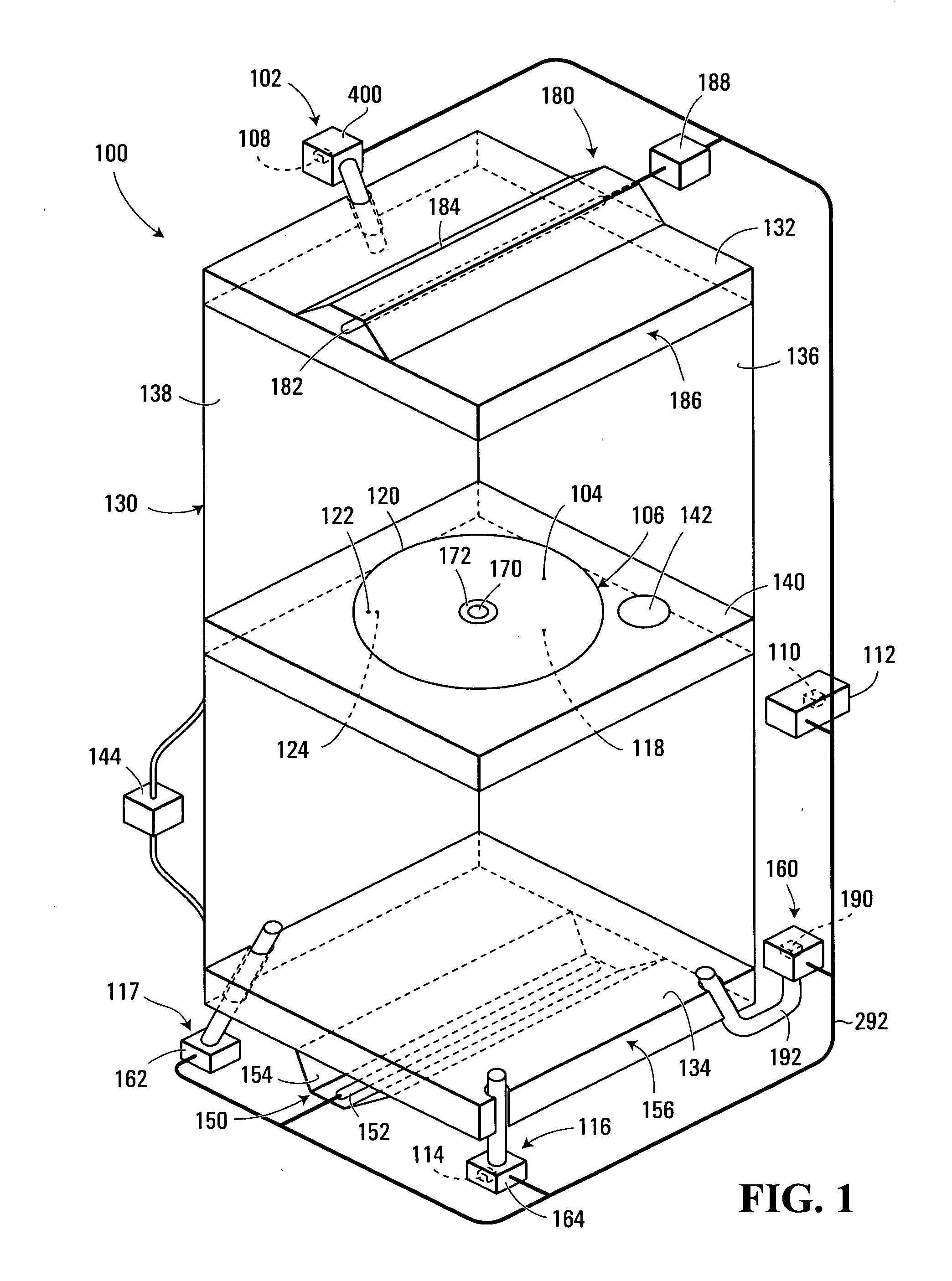
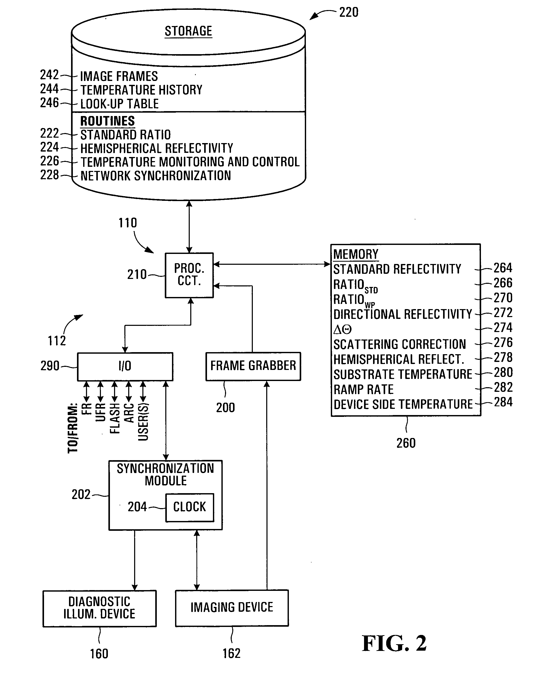
[0044] Referring to FIG. 1, a temperature measurement system according to the invention is shown generally at 100. In this embodiment, the system 100 includes a measurement device 102 configured to measure a present intensity of radiation thermally emitted from a first surface 104 of a workpiece 106. The system 100 further includes at least one processor circuit in communication with the measurement device 102. The at least one processor circuit is configured to identify a present temperature of the first surface 104, in response to the present intensity and at least one previous thermal property of the first surface at a respective previous time.

[0045] In this embodiment, the at least one processor circuit includes a processor circuit 108. In the present embodiment, the processor circuit 108 is located within a housing of the measurement device 102, although alternatively, the processor circuit may be located remotely from the measurement device if desired. In this embodiment, the ...

second embodiment

[0165] For example, referring to FIG. 11, a power control circuit of the power control system 188 according to the invention is shown generally at 970. The capacitor bank that is to be discharged to produce the irradiance flash is again symbolically shown as a single capacitor 962, for ease of illustration. Along a first electrical pathway 972 connecting one plate of the capacitor 962 to one electrode of the flash lamp, a switch 974 and an inductor 976 are interposed in series. A second electrical pathway 978 connects the other plate of the capacitor to the other electrode of the flash lamp. A resistor 980 and a second switch 982 in series, are connected between the first electrical pathway 972 and the second electrical pathway 978, with the resistor being connected to the first electrical pathway 972 at a point 984 between the first switch 974 and the inductor 976, and the second switch 986 being connected to the second electrical pathway 978 at a point 986. The second switch 982 m...

third embodiment

[0166] Similarly, referring to FIG. 12, a power control circuit of the power control system 188 according to the invention is shown generally at 990. The capacitor bank that is to be discharged to produce the irradiance flash is again symbolically shown as a single capacitor 962, for ease of illustration. Along a first electrical pathway 991 connecting a first plate of the capacitor 962 to a first electrode of the flash lamp 182, a first switch 992, a first inductor 993, and a second inductor 994 in parallel with a second switch 995, are interposed in series. In this regard, the second switch 995 is interposed along an electrical sub-pathway 996 of the first electrical pathway 991. One end of the electrical sub-pathway 996 is connected to a point 997 interposed between the first inductor 993 and the second inductor 994. The other end of the electrical sub-pathway 996 is connected to a point 998 interposed between the second inductor 994 and the first plate of the flash lamp 182. The...


PUM

PropertyMeasurementUnit
temperatureaaaaaaaaaa
diameteraaaaaaaaaa

Abstract

Temperature measurement and heat-treating methods and systems. One method includes identifying a temperature of a first surface of a workpiece, and controlling energy of an irradiance flash incident on the first surface of the workpiece, in response to the temperature of the first surface. Identifying may include identifying the temperature of the first surface during an initial portion of the irradiance flash, and controlling may include controlling the power of a remaining portion of the irradiance flash. The first surface of the workpiece may include a device side of a semiconductor wafer.

Description

CROSS-REFERENCE TO RELATED APPLICATIONS [0001] This application is a continuation of U.S. patent application Ser. No. 10 / 497,447 which was filed on Jun. 1, 2004 and was accorded a 35 U.S.C. § 371 date of Nov. 8, 2004, and which is a national stage of Patent Cooperation Treaty international application no. PCT / CA02 / 01987 filed Dec. 23, 2002, which claims the benefit of priority from U.S. patent application Ser. No. 60 / 342,115 filed Dec. 26, 2001. Each of the above-referenced applications is hereby incorporated herein by reference.FIELD OF THE INVENTION [0002] Aspects of the present invention relate to methods and systems for temperature measurement. Further aspects of the invention relate to methods and systems for heat-treating a workpiece. BACKGROUND OF THE INVENTION [0003] In some applications, it is necessary to determine the temperature of a workpiece whose temperature is difficult to directly measure. For example, where the workpiece is a semiconductor wafer, although the tempe...

Claims


Application Information

Patent Timeline
Patent Type & Authority Applications(United States)
IPC IPC(8): C21D1/09G01J5/00G01J5/10G01J5/48H01L21/00
CPCG01J5/0003G01J5/10H01L21/67115H01L21/67248H01L21/67276G01J5/00H01L21/00
Inventor CAMM, DAVID M.KERVIN, SHAWNALEFRANCOIS, MARCEL EDMONDSTUART, GREG
Owner MATTSON TECHNOLOGY
Why Eureka
Try Eureka