Multi bits flash memory device and method of operating the same

a multi-bit, flash memory technology, applied in semiconductor devices, digital storage, instruments, etc., can solve the problem that the 2-dimentional devices are not suitable for multi-bit operation more, and achieve the effect of improving the stability and reliability of the devi

Inactive Publication Date: 2006-05-11
SAMSUNG ELECTRONICS CO LTD
View PDF3 Cites 26 Cited by
  • Summary
  • Abstract
  • Description
  • Claims
  • Application Information

AI Technical Summary

Benefits of technology

[0010] The present invention provides a multi bits flash memory device with a memory cell structure capable of storing more than 2 bits.

Problems solved by technology

However, 2-dimentional devices are not suitable for multi-bit operation more than 3 bits in performing program, erase and read operations.

Method used


Image

  • Multi bits flash memory device and method of operating the same
  • Multi bits flash memory device and method of operating the same
  • Multi bits flash memory device and method of operating the same

Examples


Embodiment Construction

[0029] The present invention will now be described more fully with reference to the accompanying drawings, in which exemplary embodiments of the invention are shown. The invention may, however, be embodied in many different forms and should not be construed as being limited to the embodiments set forth herein; rather, these embodiments are provided so that this disclosure will be thorough and complete, and will fully convey the concept of the invention to those skilled in the art.

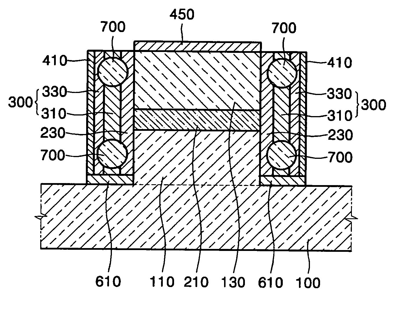
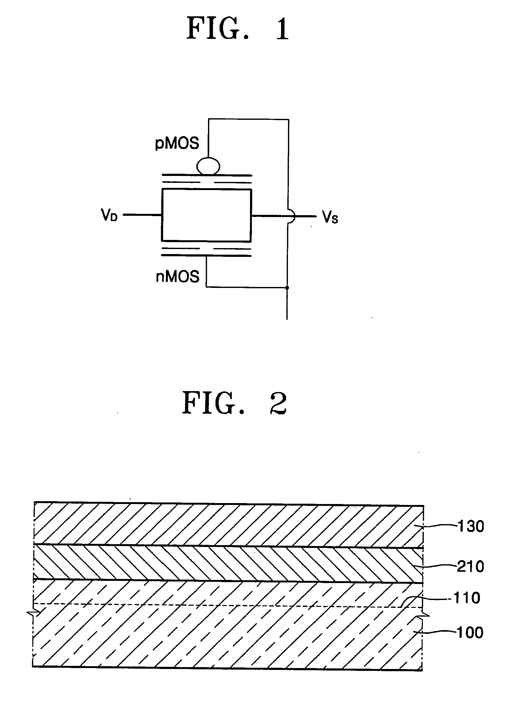
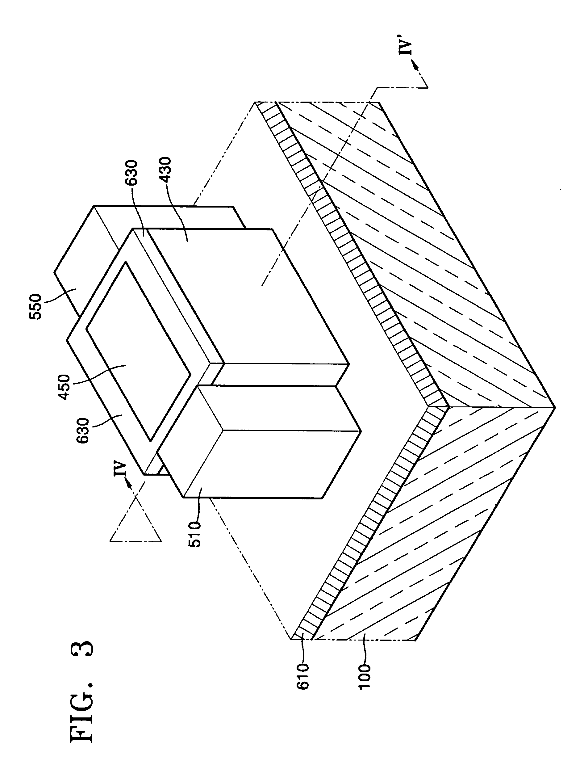
[0030] A 3-dimentional multi bits flash memory device according to embodiment of the present invention includes two active layers and an active interlayer isolation layer interposed therebetween. The active layers and the active interlayer isolation layer form a stacked structure in the form of a hexahedron. A source, a drain, and gates formed on side surfaces of the stacked structure. A channel is formed in each of the active layers, and the active interlayer isolation layer is used as an insulator. A com...


PUM


Abstract

A multi bits flash memory device and a method of operating the same are disclosed. The multi bits flash memory device includes: a stacked structure including: a first active layer with a mesa-like form disposed on a substrate; a second active layer, having a different conductivity type from the first active layer, formed on the first active layer; an active interlayer isolation layer interposed between the first active layer and the second active layer such that the first active layer is electrically isolated from the second active layer; a common source and a common drain formed on a pair of opposite side surfaces of the stacked structure; a common first gate and a common second gate formed on the other pair of opposite side surfaces of the stacked structure; a tunnel dielectric layer interposed between the first and second gates and the first and second active layers; and a charge trap layer, storing charges that tunnel through the tunnel dielectric layer, interposed between the tunnel dielectric layer and the first and second gates.

Description

BACKGROUND OF THE INVENTION [0001] This application claims the benefit of Korean Patent Application No. 10-2004-0090892, filed on Nov. 9, 2004, in the Korean Intellectual Property Office, the disclosure of which is incorporated herein in its entirety by reference. [0002] 1. Field of the Invention [0003] The present invention relates to a semiconductor device, and more particularly, to a multi bits flash memory device using a complementary metal oxide semiconductor (CMOS) and a method of operating the same. [0004] 2. Description of the Related Art [0005] In order to increase memory density, the sizes of memory cells can be reduced. Alternatively, memory density can be increased by increasing the number of possible states of charges in each memory cell. For example, it is reported a flash memory cell having multi floating gates that can assume 4 states and, therefore, store 2 bits simultaneously. [0006] However, memory cells have often been embodied in two dimension-structures. Two-di...

Claims


Application Information

Patent Timeline
Patent Type & Authority Applications(United States)
IPC IPC(8): H01L29/76H01L21/336
CPCB82Y10/00G11C11/5607G11C11/5621G11C11/5628G11C11/5657G11C13/025H01L21/28273H01L21/28282H01L21/28291H01L29/0692H01L29/4232H01L29/7923H01L29/40114H01L29/40117H01L29/40111
Inventor KIM, WON-JOOPARK, YOON-DONGLEE, EUN-HONGSEO, SUN-AESHIN, SANG-MINLEE, JUNG-HOONCHANG, SEUNG-HYUK
Owner SAMSUNG ELECTRONICS CO LTD
Why Eureka
Try Eureka