Semiconductor chip capable of implementing wire bonding over active circuits

a technology of active circuit and semiconductor, applied in the direction of semiconductor devices, semiconductor/solid-state device details, electrical apparatus, etc., can solve the problems of unfavorable chip size shrinkage, unfavorable /b> and lower active circuits, and bonding pads which spread around on the chip, so as to reduce mechanical stresses pressing on the top interconnection metal layer directly during bonding and reduce the effect of wiring area and chip size shrinkag

Active Publication Date: 2006-05-11
UNITED MICROELECTRONICS CORP
View PDF10 Cites 21 Cited by
  • Summary
  • Abstract
  • Description
  • Claims
  • Application Information

AI Technical Summary

Benefits of technology

[0009] Since the BOAC integrated circuit structure of the present invention further includes the stress-buffering dielectric between the bondable metal pad and the top interconnection metal layer, mechanical stresses pressing on the top interconnection metal layer directly during bonding will be reduced. Additionally, the integrated circuit will not be damaged. In the present invention, since the first via plug linking the bondable metal pad with the top interconnection metal layer and the second via plug linking the bonding pad structure with the interconnection metal layer beneath the bondable metal pad are disposed beneath the bondable metal pad, the wiring area will be diminished and the chip size will be shrunk. Moreover, since the wire between the bondable metal pad and the lower active circuit of the present invention is shorter, the electric characteristics will be better.

Problems solved by technology

Therefore, bonding pads which spread around on a chip are obstacles for reducing the chip size.
Moreover, the outside wire, which is formed for electrically linking the top interconnection metal layer 52 and the lower active circuits, is unfavorable for chip size shrinkage.

Method used


Image

  • Semiconductor chip capable of implementing wire bonding over active circuits
  • Semiconductor chip capable of implementing wire bonding over active circuits
  • Semiconductor chip capable of implementing wire bonding over active circuits

Examples


Embodiment Construction

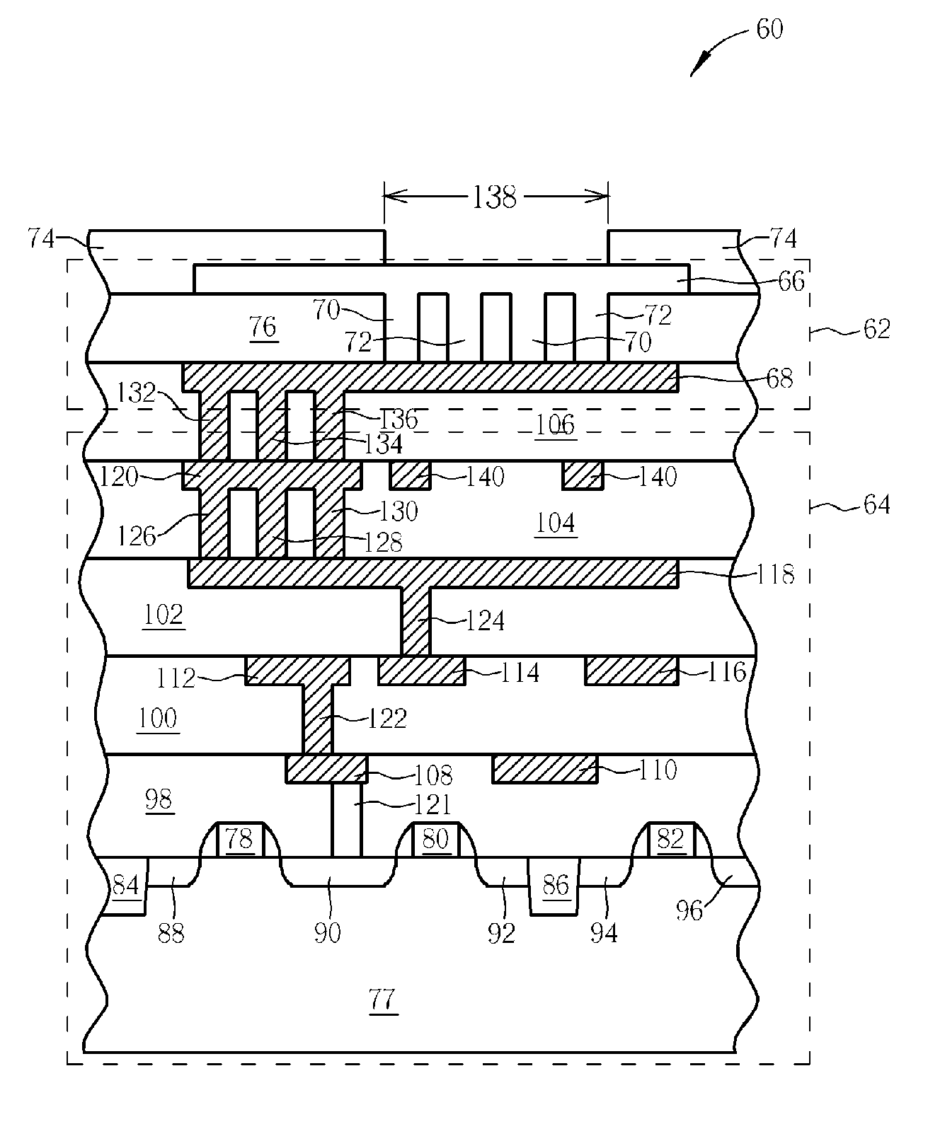
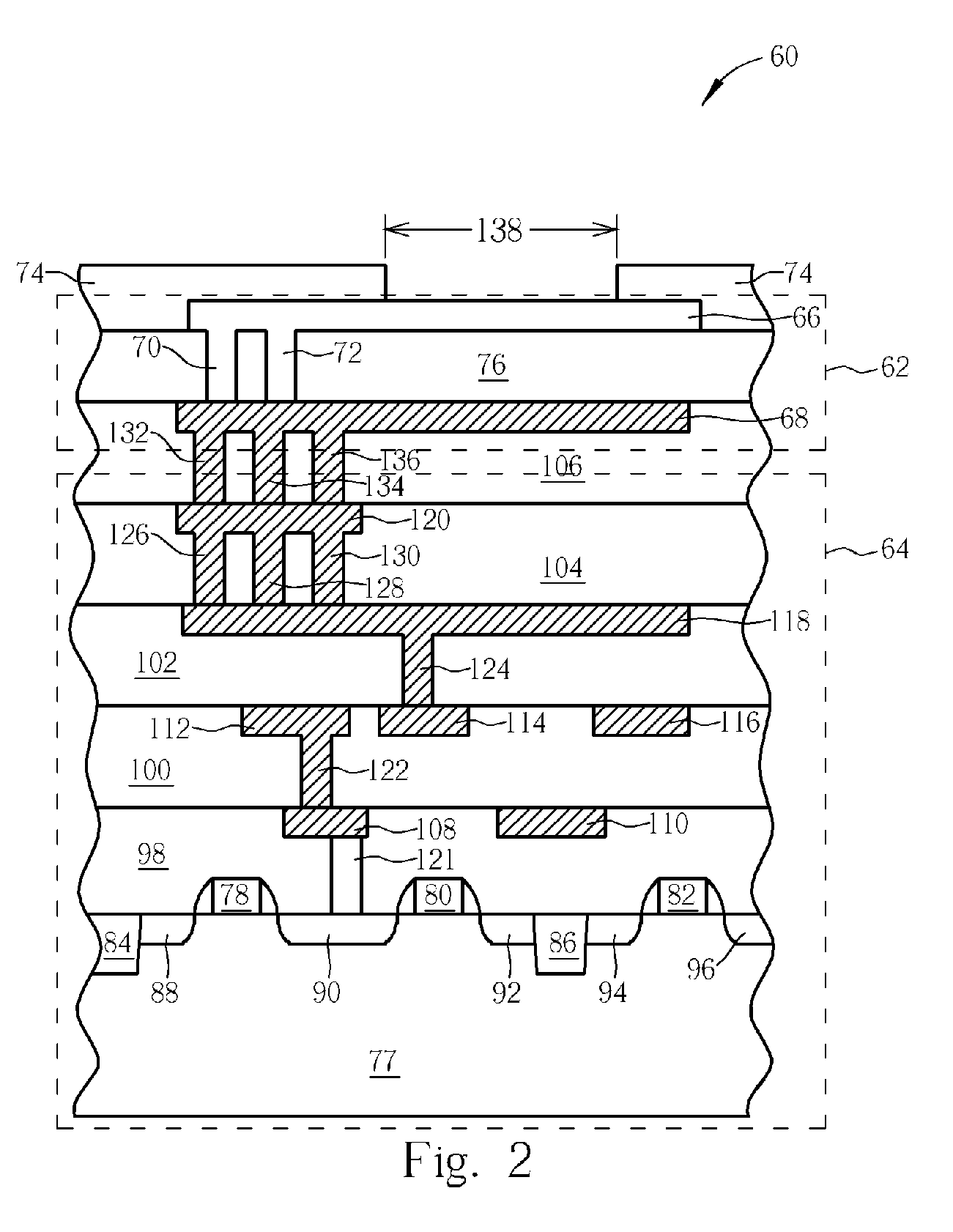
[0015] Please refer to FIG. 2. FIG. 2 is a schematic cross-sectional diagram of a BOAC integrated circuit structure according to a first embodiment of the present invention. As shown in FIG. 2, a BOAC integrated circuit structure 60 of the present invention includes a bonding pad structure 62 and an active circuit region 64. The bonding pad structure 62 further includes a bondable metal pad 66, a top interconnection metal layer 68, first via plugs 70 and 72 located beneath a section of the bondable metal pad 66 that is covered by a protection layer 74 and electrically linking the bondable metal pad 66 with the top interconnection metal layer 68, and a stress-buffering dielectric 76 located between the bondable metal pad 66 and the top interconnection metal layer 68.

[0016] The active circuit region 64 may include input / output (I / O) devices / circuits or electrostatic discharge (ESD) devices / circuits on a semiconductor substrate 77, and are made up of metal-oxide-semiconductor field-ef...


PUM


Abstract

A semiconductor chip capable of implementing wire bonding over active circuits (BOAC) is provided. The semiconductor chip includes a bonding pad structure which includes a bondable metal pad, a top interconnection metal layer, a stress-buffering dielectric, and at least a first via plug between the bondable metal pad and the top interconnection metal layer. The semiconductor chip also includes at least an interconnection metal layer, at least a second via plug between the interconnection metal layer and the bonding pad structure, and an active circuit situated underneath the bonding pad structure on a semiconductor bottom.

Description

BACKGROUND OF INVENTION [0001] 1. Field of the Invention [0002] The present invention relates to the field of semiconductor integrated circuits, and more particularly, to a semiconductor chip capable of implementing wire bonding over active circuits (also referred to as “BOAC”). [0003] 2. Description of the Prior Art [0004] Accompanying progress of the semiconductor technology, critical dimensions of integrated circuits are continually shrunk. Therefore, bonding pads which spread around on a chip are obstacles for reducing the chip size. For this reason, implementing wire bonding over active circuits is a trend for chips design and manufacturing. [0005]FIG. 1 is a schematic cross-sectional diagram of a BOAC integrated circuit structure according to the prior art. As shown in FIG. 1, a BOAC integrated circuit structure 10 of the prior art has a plurality of active circuits on a semiconductor substrate 12. The plurality of active circuits include input / output (I / O) devices / circuits or...

Claims


Application Information

Patent Timeline
Patent Type & Authority Applications(United States)
IPC IPC(8): H01L23/52H01L23/48
CPCH01L23/53228H01L24/05H01L2224/02166H01L2224/05093H01L2224/05095H01L2224/05624H01L2924/01013H01L2924/01014H01L2924/01029H01L2924/05042H01L2924/13091H01L2924/14H01L2924/00014H01L2924/01033
Inventor WU, BING-CHANGWANG, KUN-CHIHCHAO, MEI-LINGCHEN, SHIAO-SHIEN
Owner UNITED MICROELECTRONICS CORP
Why Eureka
Try Eureka